Thin-film transistor device and method of manufacturing the same

a technology of thin film transistors and transistors, which is applied in the direction of semiconductor/solid-state device manufacturing, semiconductor devices, electrical devices, etc., can solve the problems of insufficient mobility in the channel, insufficient on-current, and insufficient carrier mobility, so as to reduce the effect of widening the depletion layer, increase the current value, and increase the current valu

Inactive Publication Date: 2012-02-09
PANASONIC LIQUID CRYSTAL DISPLAY CO LTD +1
View PDF1 Cites 3 Cited by
  • Summary
  • Abstract
  • Description
  • Claims
  • Application Information

AI Technical Summary

Benefits of technology

[0011]Since the thin-film transistor device according to an aspect of the present invention has a structure in which the source electrode and the drain electrode are in direct contact with a channel layer, and the thickness of the source electrode and the drain electrode is less than the thickness of the channel layer, the thin-film transistor device is capable of reducing the effect of the widening of the depletion layer formed by a schottky barrier, and increasing the current at a linear region of the electrical characteristics of a TFT. As a result, it is possible to increase the current value at a linear region of the electrical characteristics of the TFT, in a top gate thin-film transistor device.

Problems solved by technology

However, when amorphous silicon is used in the channel layer, sufficient mobility cannot be obtained in the channel, and thus sufficient on-current cannot be obtained.
Although, in the thin-film transistor device described in Patent Reference 1, a polycrystalline silicon (P-Si) layer is provided adjacent to an amorphous hydrogenated silicon (a-Si:H) layer in the channel layer, sufficient carrier mobility cannot be obtained even with such configuration.

Method used


Image

  • Thin-film transistor device and method of manufacturing the same
  • Thin-film transistor device and method of manufacturing the same
  • Thin-film transistor device and method of manufacturing the same

Examples


Embodiment Construction

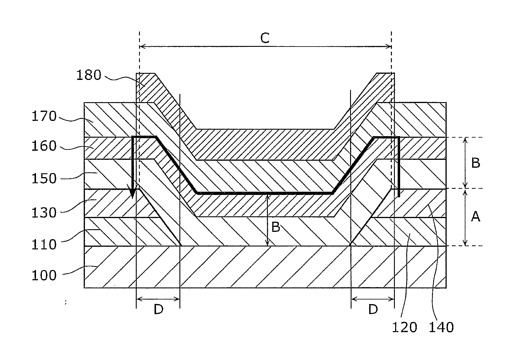
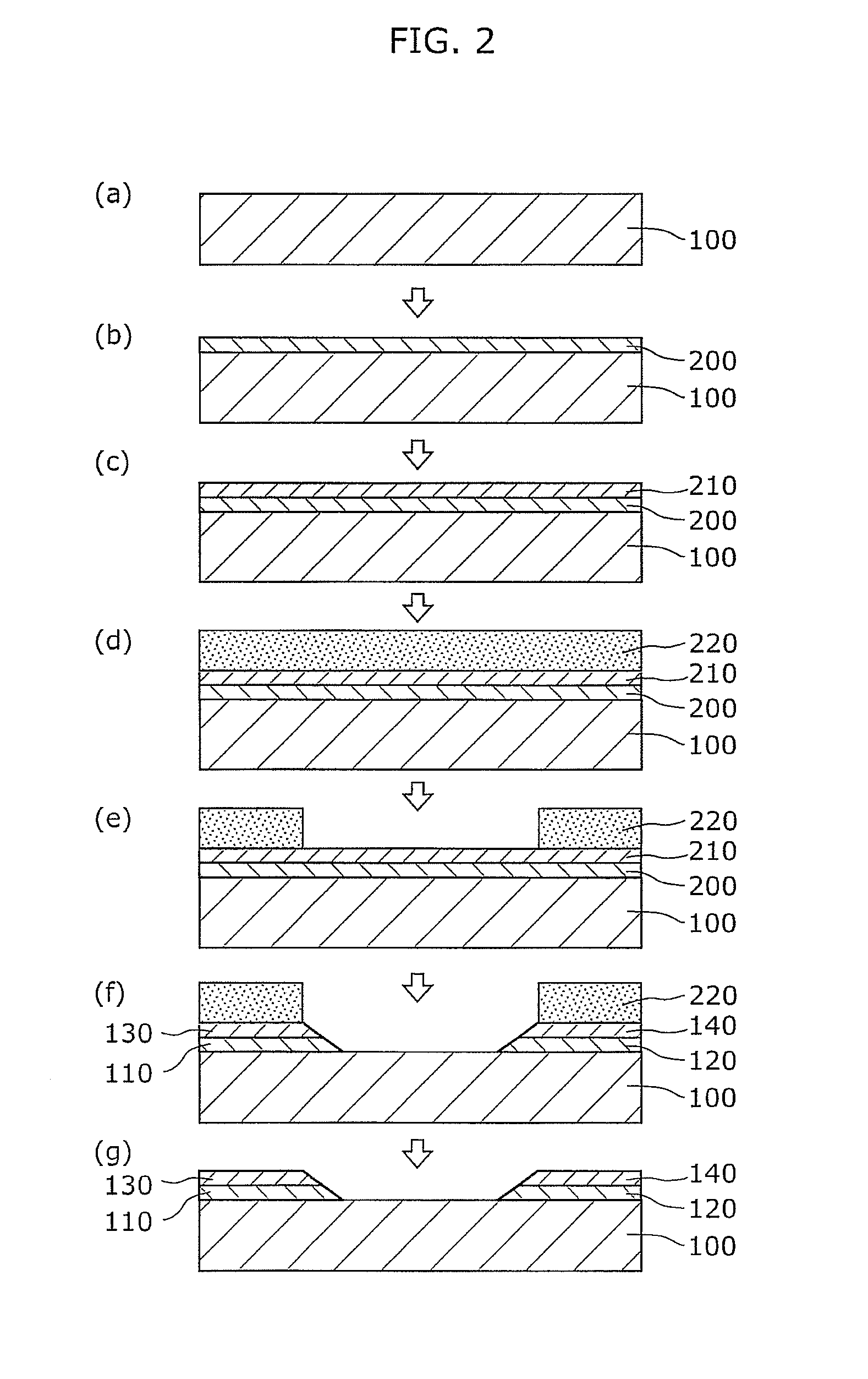
[0030]In order to achieve the aforementioned object, the thin-film transistor device according to an aspect of the present invention is characterized in including: a substrate; a source electrode and a drain electrode formed on the substrate; silicon layers, one of which is stacked within a top surface region of the source electrode and an other of which is stacked within a top surface of the drain electrode, the silicon layers being amorphous and doped with an impurity; a first channel layer formed continuously (i) on the substrate, in a region between the source electrode and the drain electrode, (ii) on a side surface of each of the source electrode and the drain electrode, and (iii) on a side surface and a top surface of each of the silicon layers, the first channel layer being made of an amorphous silicon layer; a second channel layer stacked on the first channel layer and made of one of a polysilicon layer and a microcrystalline silicon layer, the second channel layer being fo...


PUM


Abstract

In the thin-film transistor device: the stacked thickness of either a source electrode or a drain electrode and a corresponding one of silicon layers is the same value or a value close to the same value as the stacked thickness of a first channel layer and a second channel layer; the stacked thickness of the first channel layer and the second channel layer is the same in a region between the source electrode and the drain electrode and above the source electrode and the drain electrode; the first channel layer and the second channel layer are sunken in the region between the source electrode and the drain electrode, following a shape between the source electrode and the drain electrode; and the gate electrode has one region overlapping with the source electrode and an other region overlapping with the drain electrode.

Description

CROSS REFERENCE TO RELATED APPLICATION[0001]This is a continuation application of PCT application No. PCT / JP2011 / 001582 filed on Mar. 17, 2011, designating the United States of America.BACKGROUND OF THE INVENTION[0002](1) Field of the Invention[0003]The present invention relates to thin-film transistor devices and methods of manufacturing the same, and relates particularly to a thin-film transistor device for driving and for switching in an organic electroluminescence (EL) display device and a liquid crystal display device, and to a method of manufacturing the same.[0004](2) Description of the Related Art[0005]In electronic devices, such as television receivers, which use an organic electroluminescence (EL) display device or a liquid crystal display device, luminescence elements which are arranged in a matrix and configure the organic EL display device or the liquid crystal display are driven by thin-film transistor (TFT) devices.[0006]Top gate (staggered) thin-film transistor devic...

Claims


Application Information

Patent Timeline
Patent Type & Authority Applications(United States)
IPC IPC(8): H01L33/08H01L21/336
CPCH01L29/41733H01L29/66757H01L29/78696H01L29/78666H01L29/78675H01L29/78636H01L29/04
Inventor NAGAI, HISAOHOTTA, SADAYOSHIKAWACHI, GENSHIRO
Owner PANASONIC LIQUID CRYSTAL DISPLAY CO LTD
Why Eureka
Try Eureka