
Display Device And Display Control Method
a display device and control method technology, applied in the field of display devices and display control methods, can solve the problems of output luminance, output luminance, output luminance differences among leds due to variation in deterioration property, etc., and achieve the reduction of luminance over an entire screen, correct luminance non-uniformity, and loss of display gray scales
- Summary
- Abstract
- Description
- Claims
- Application Information
AI Technical Summary
Benefits of technology
Problems solved by technology
Method used
Image

Examples
example 1
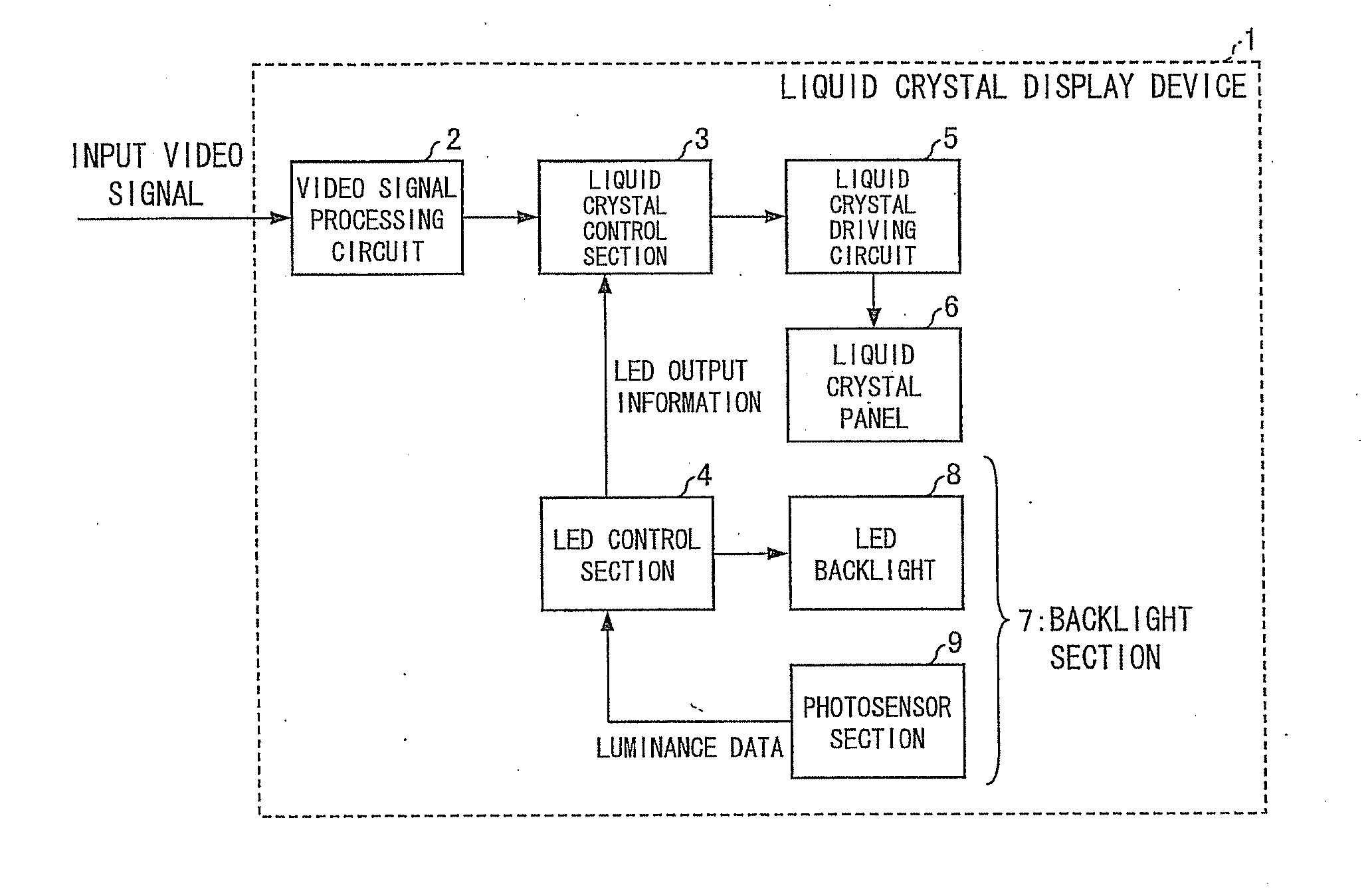
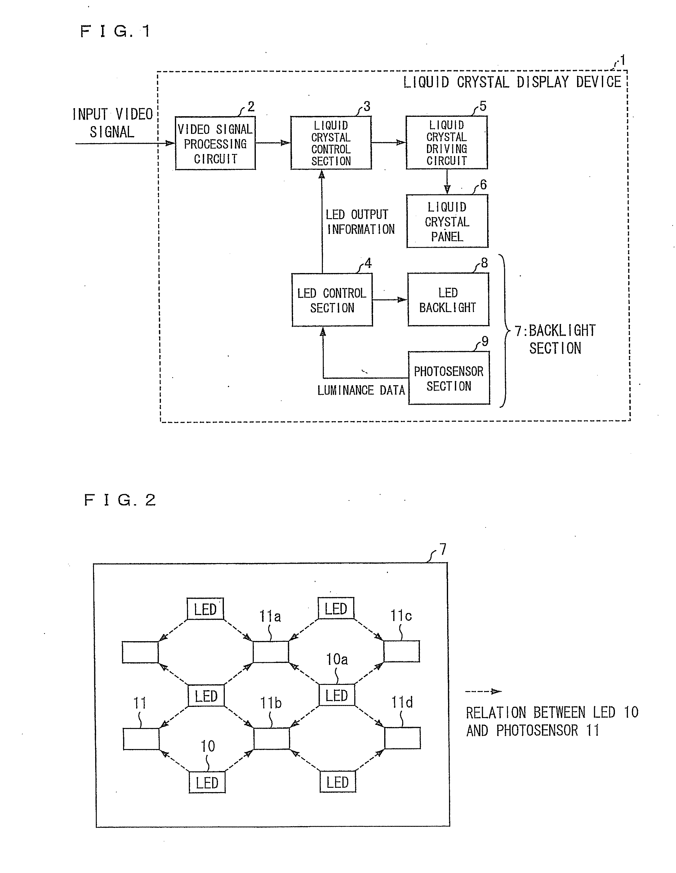
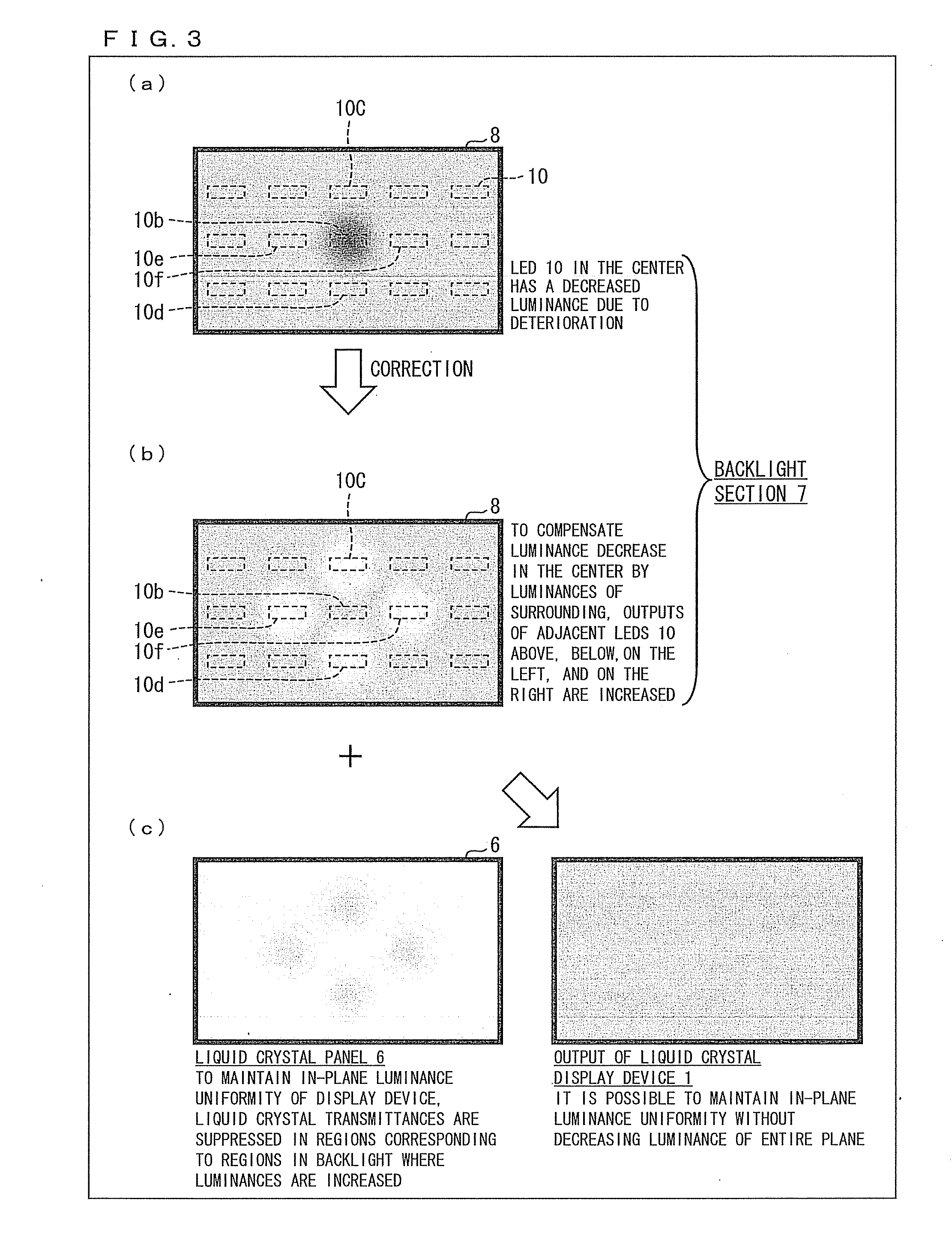
[0053]FIG. 1 is a block diagram of a liquid crystal display device (display device) 1 in accordance with Example 1. The liquid crystal display device 1 includes a video signal processing circuit (video signal processing section) 2, a liquid crystal control section (display control section) 3, an LED control section (light-emitting element control section) 4, a liquid crystal driving circuit 5, a liquid crystal panel (display panel) 6, and a backlight section 7. A plurality of pixels are arranged in the liquid crystal panel 6. The backlight section 7 includes (i) an LED backlight 8, in which a plurality of LEDs (light-emitting elements) 10 (see FIG. 2) are provided and (ii) a photosensor section 9, in which a plurality of photosensors 11 (see FIG. 2) are provided.
[0054]The liquid crystal display device 1 employs the LED backlight 8, which is a direct backlight in which the plurality of LEDs 10 are arranged in a matrix manner. Note that the liquid crystal display device 1 does not car...
example 2
[0089]Another example of the present invention will be described below with reference to FIGS. 5 and 6. Note that configurations of Example 2 other than configurations to be described in Example 2 are the same as those of early-described Example 1. For easy explanation, the same reference signs will be given to members each having the same function as a member illustrated in the figures of Example 1, and descriptions on such a member will be omitted.
[0090]FIG. 5 is a block diagram showing a liquid crystal display device 12 in accordance with Example 2. The liquid crystal display device 12 is different from the liquid crystal display device 1 illustrated in FIG. 1 in that an area active driving circuit (area driving section) 13 is provided. The area active driving circuit 13 supplies, to the LED control section 4, output luminances modulated in accordance with levels of video signals to be supplied to pixels in one of a plurality of regions into which a display region, which is const...
example 3
[0121]A further example of the present invention will be described below with reference to FIGS. 7 and 8. Note that configurations of Example 3 other than configurations to be described in Example 3 are the same as those of early-described Examples 1 and 2. For easy explanation, the same reference signs will be given to members each having the same function as a member illustrated in the figures of Examples 1 and 2, and descriptions on such a member will be omitted.
[0122]FIG. 7 is a block diagram showing a liquid crystal display device 23 in accordance with Example 3. The liquid crystal display device 23 is different from the liquid crystal display device 12 illustrated in FIG. 2 in that (i) no liquid crystal control section 3 and no LED control section 4 are provided and (ii) an LED correcting section (light-emitting element correcting section) 24 is provided in the LED data calculation section 16.
[0123]In the liquid crystal display device 23 illustrated in FIG. 7, the LED correcti...
PUM
 Abstract
Description
Claims
Application Information