Display device and electronic product
a technology of electronic products and display devices, applied in the field of display devices, can solve the problems of image quality failure called “burning” prone to occur, the luminance of each pixel in the organic el display is deteriorated with time, and the luminance of the organic el display is reduced with lapse of time, so as to compensate the luminance deterioration of pixels, reduce the number of light sensors, and improve the effect of image quality
- Summary
- Abstract
- Description
- Claims
- Application Information
AI Technical Summary
Benefits of technology
Problems solved by technology
Method used
Image
Examples
first embodiment
[Whole Configuration of a Panel]
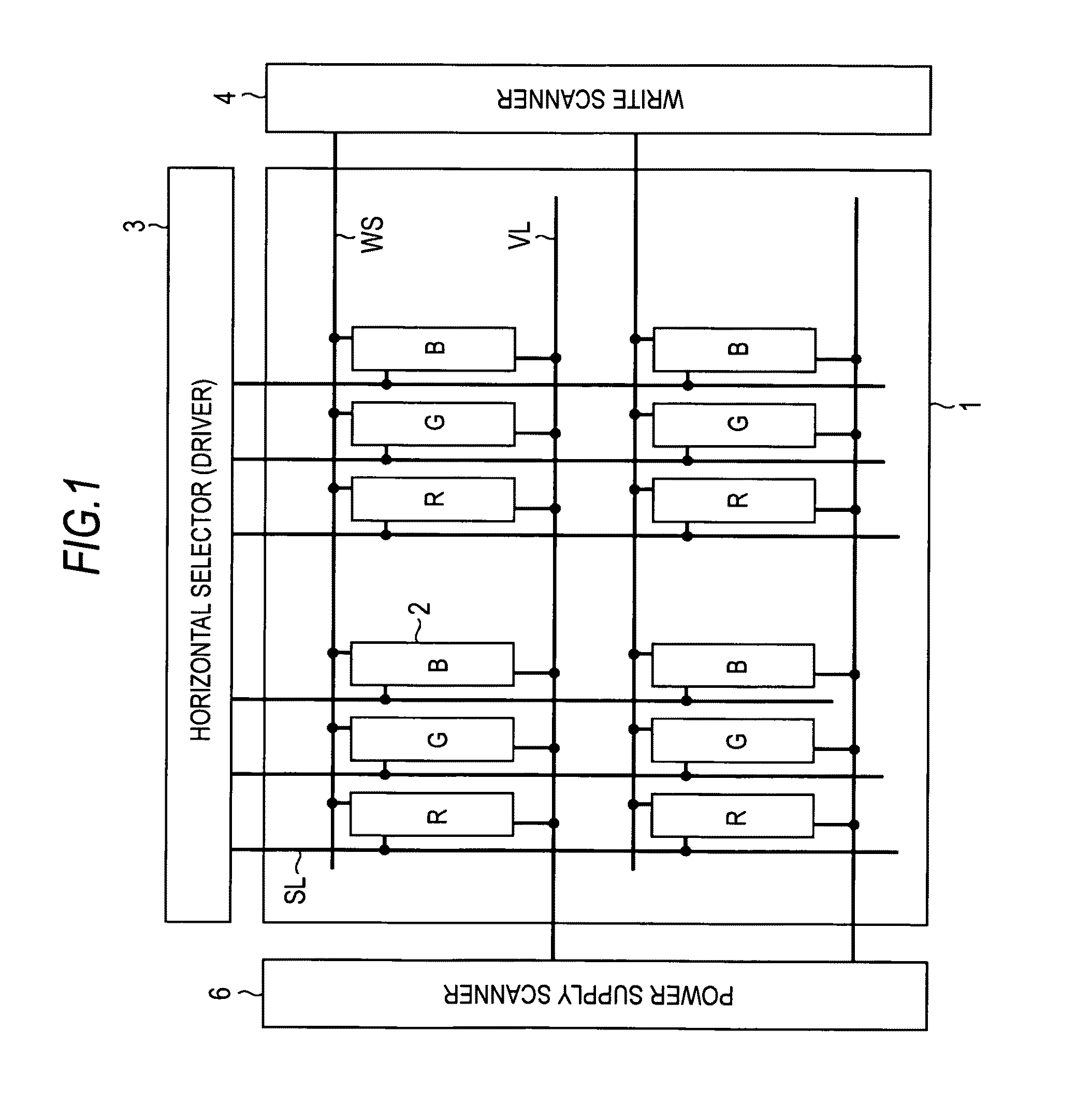
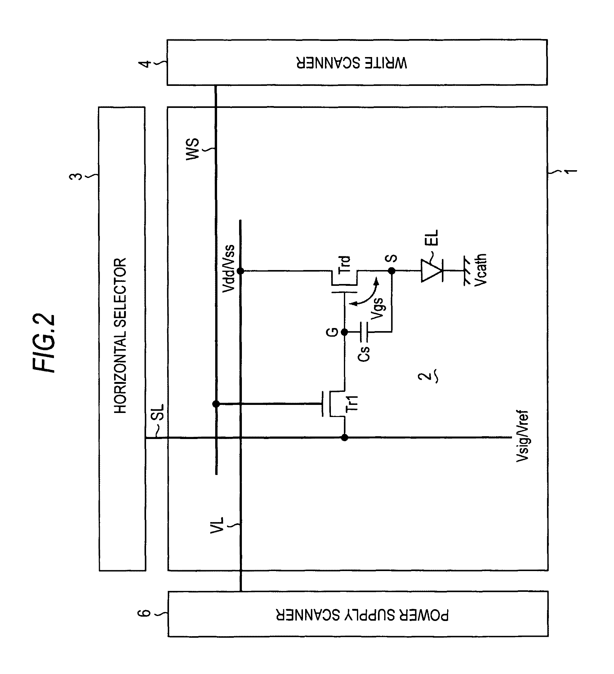
[0058]FIG. 1 is the whole configuration diagram showing a panel which is a main unit of a display device according to an embodiment of the invention. As shown in the drawing, the display device includes a pixel array unit 1 (screen unit) and a drive unit which drives the pixel array unit 1. The pixel array unit 1 has rows of scanning lines WS, columns of signal lines SL, matrix-state pixels 2 arranged at portions where the both lines intersect and feeding lines (power lines) VL arranged so as to correspond to respective lines of respective pixels 2. In the example, any of RGB three primary colors is assigned to each pixel 2 to realize color display. However, the invention is not limited to this and also includes a single-color display device. The drive unit includes a write scanner 4 performing line-sequential scanning of the pixels 2 row by row by sequentially supplying a control signal to respective scanning lines WS, a power supply scanner 6 supply...
modification example
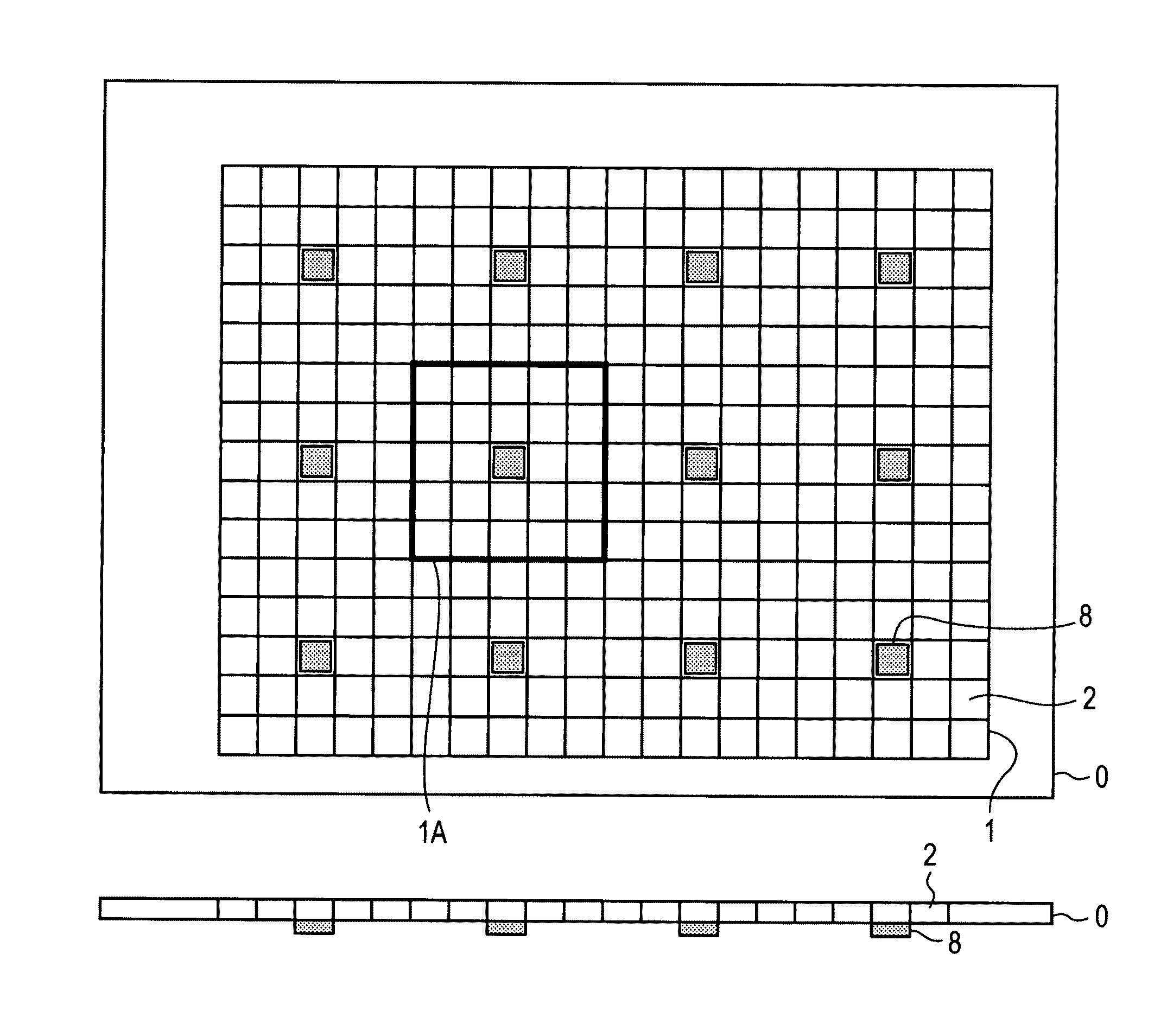
[0081]FIG. 6 is a block diagram showing a modification example of the display device according to the first embodiment shown in FIG. 5. In order to make understanding easier, corresponding reference numerals are given to portions corresponding to components shown in FIG. 5. A different point is that the light sensor 8 is arranged on the surface side, not on the reverse side of the panel “0”. When the light sensor 8 is arranged on the surface side, there is an advantage that the light receiving amount is increased as compared with the case of the reverse side. However, when the light sensor 8 is arranged on the surface side of the panel “0”, there occurs a disadvantage that light emission from part of pixels is sacrificed.
[Configuration of the Panel]
[0082]FIG. 7 is a schematic plan view and a cross-sectional view showing a configuration of the panel included in the display device shown in FIG. 5. As shown in the drawing, the screen unit (pixel array unit) 1 is arranged at the center ...
second embodiment
Operations of Second Embodiment
[0100]FIG. 14A is a timing chart showing operations of the display device according to the second embodiment. In the second embodiment, the accuracy of the burn-in correction is increased by improving variations in the accuracy of the burn-in correction described above. FIG. 14A represents a dot-sequential scanning for lighting only pixels of measurement targets. As described above, the dot-sequential scanning is performed in the same sequence as that of the normal video display operations shown in FIG. 3. That is, after the Vth correction is performed, the video signal in the given level is written in the pixel of the measurement target and the mobility correction is performed, then, the pixel is allowed to emit light.
[0101]The timing chart shown in FIG. 14A indicates a case in which the pixel of the measurement target is close to the light sensor. In this case, the light sensor can obtain a sufficient amount of received light from the pixel of the me...
PUM
 Abstract
Description
Claims
Application Information


