Display device and electronic product

Active Publication Date: 2010-05-13
JOLED INC
View PDF23 Cites 20 Cited by
  • Summary
  • Abstract
  • Description
  • Claims
  • Application Information

AI Technical Summary

Benefits of technology

[0019]Particularly, in the embodiment of the invention, the screen unit is sectioned and the light sensor is arranged with respect to each section. Each section includes a number of pixels in a range in which the corresponding light sensor can detect light emitting luminance. According to the embodiment of the invention, it is not necessary to provide light sensors so as to correspond to respective pixels for detecting light emitting luminance of each pixel, therefore, the necessary number of light sensors can be drastically reduced, as a result, it is possible to simplify a display panel structure as well as to reduce costs for the display panel.
[0020]Furthermore, in a display device accordi

Problems solved by technology

In the light emitting element, current/luminance characteristics tend to deteriorate with time.
Accordingly, there is a problem that luminance of each pixel in the organic EL display is reduced with

Method used


Image

  • Display device and electronic product
  • Display device and electronic product
  • Display device and electronic product

Examples


modification example

[0089]FIG. 6 is a block diagram showing a modification example of the display device according to the first embodiment shown in FIG. 5. In order to make understanding easier, corresponding reference numerals are given to portions corresponding to components shown in FIG. 5. A different point is that the light sensor 8 is arranged on the surface side, not on the reverse side of the panel “0”. When the light sensor 8 is arranged on the surface side, there is an advantage that the light receiving amount is increased as compared with the case of the reverse side. However, when the light sensor 8 is arranged on the surface side of the panel “0”, there occurs a disadvantage that light emission from part of pixels is sacrificed.

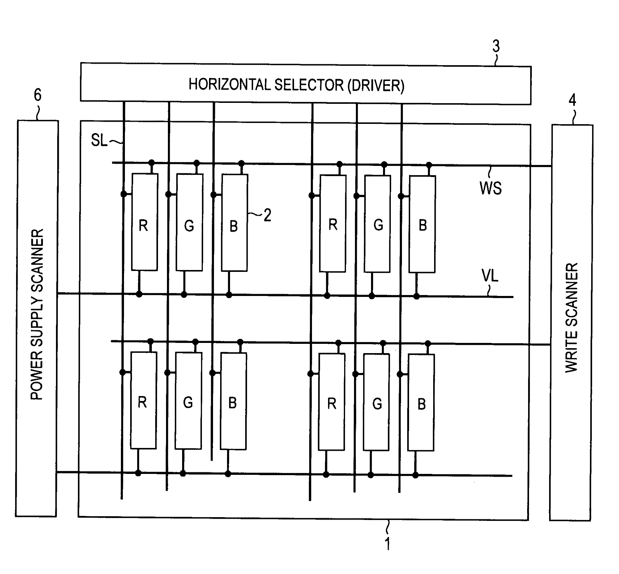
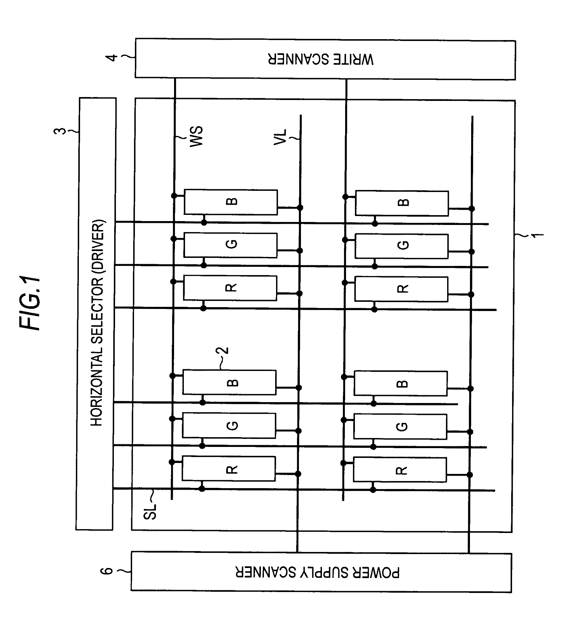
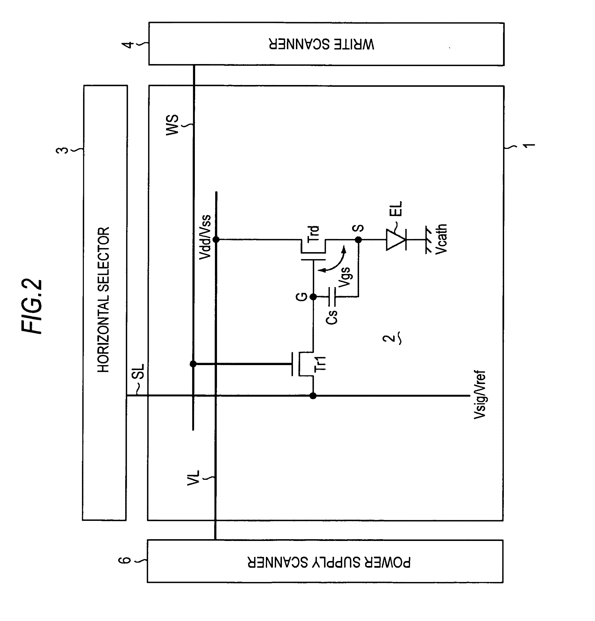
Configuration of the Panel

[0090]FIG. 7 is a schematic plan view and a cross-sectional view showing a configuration of the panel included in the display device shown in FIG. 5. As shown in the drawing, the screen unit (pixel array unit) 1 is arranged at the center of...

first embodiment

Specific Configuration of First Embodiment

[0113]FIGS. 13A and 13B are schematic diagrams representing specific configurations of a display device according to the first embodiment of the invention. FIG. 13A is a reference example cited for comparison, which represents parallel drive of plural sensors. As shown in the drawing, the screen unit 1 (pixel array unit) 1 is formed in the panel “0”. The screen unit 1 is sectioned into plural regions. On the reverse side of the panel “0”, plural light sensors 8 are arranged so as to correspond to plural regions. The plural light sensors 8 are driven in parallel in one frame. The plural light sensors are connected to the signal processing unit (DSP) 10 through wirings respectively. The DSP 10 includes, for example, an ASIC chip, in which connection pins are necessary for the number of plural light sensors 8. However, when the number of light sensors 8 is increased, the number of pins is not actually sufficient in a general-purpose ASIC chip a...

second embodiment

[Configuration]

[0123]FIG. 16 is a schematic block diagram showing a second embodiment. A display device according to the second embodiment basically includes a screen unit, a drive unit and a signal processing unit (DSP) 10. The screen unit (not shown) has a panel including rows of scanning lines, columns of signal lines, matrix-state pixels arranged at portions where respective scanning lines and respective signal lines intersect and a light sensor. The drive unit (not shown) includes a scanner sequentially supplying a control signal to respective scanning lines and a driver supplying a video signal to respective signal lines. The pixel (not shown) takes a video signal from the signal line as well as emits light in accordance with the taken video signal when selected in accordance with the control signal supplied from the scanning line. The light sensor detects light emitting luminance of each pixel and outputs a corresponding luminance signal. The signal processing unit 10 correct...


PUM


Abstract

A display device includes: a screen unit; a drive unit; a signal processing unit; and a selector, wherein the screen unit includes rows of scanning lines, columns of signal lines, matrix-state pixel circuits and a light sensor, the drive unit includes a scanner supplying a control signal to the scanning lines and a driver supplying a video signal to the signal lines, the screen unit is sectioned into plural regions each having plural pixel circuits, the pixel circuit emits light in accordance with the video signal, the light sensor is arranged with respect to each region and outputs a luminance signal in accordance with the light emission, the selector supplies plural luminance signals to the signal processing unit by switching the signals, and the signal processing unit corrects the video signal in accordance with the luminance signals and supplies the video signal to the driver.

Description

BACKGROUND OF THE INVENTION[0001]1. Field of the Invention[0002]The present invention relates to a display device displaying images by current-driving a light emitting element arranged at each pixel. The invention also relates to an electronic product using the display device. Particularly, the invention relates to a drive system of a so-called active matrix display device, which controls a current amount flowing in the light emitting element such as an organic EL element by an insulated-gate field effect transistor provided in each pixel circuit.[0003]2. Description of the Related Art[0004]In display devices, for example, in a liquid crystal display, a large number of pixels are arranged in a matrix state and images are displayed by controlling transmission intensity or reflection intensity of incident light in each pixel in accordance with image information to be displayed. This is the same as in an organic EL display in which organic EL elements are used for pixels, however, the ...

Claims


Application Information

Patent Timeline
IPC IPC(8): G06F3/038G09G3/20H05B44/00
CPCG09G3/3233G09G2320/045G09G3/30G09G2360/145G09G2360/147G09G2320/046
Inventor YAMASHITA, JUNICHIUCHINO, KATSUHIDE
Owner JOLED INC
Why Eureka
Try Eureka