Display device and electronic product

a technology of electronic products and display devices, applied in the field of display devices, can solve the problems of image quality failure called “burning” prone to occur, the luminance of each pixel in the organic el display is reduced with lapse of time, and the current/luminance characteristics tend to deteriorate with time, so as to achieve the effect of reducing the number of light sensors, reducing the detection time of light emitting luminance, and reducing the total detection tim

Inactive Publication Date: 2014-08-19
JOLED INC
View PDF16 Cites 0 Cited by
  • Summary
  • Abstract
  • Description
  • Claims
  • Application Information

AI Technical Summary

Benefits of technology

[0017]According to the embodiment of the invention, the signal processing unit corrects the video signal in accordance with the luminance signal outputted from the light sensor as well as supplies the corrected video signal to the driver of the drive unit. According to the configuration, it is possible to compensate luminance deterioration of pixels by the correction of the video signal, and as a result, image quality failures such as “burn-in” which have been problems from the past can be prevented.
[0019]Particularly in the embodiment of the invention, the screen unit is sectioned into plural regions in a range in which these regions do not interfere with one another. The drive unit detects light emitting luminances of plural pixels at the same time by allowing pixels belonging to different regions to emit light at the same time. Accordingly, light emitting luminances of plural pixels are detected at the same time in the embodiment of the invention, and therefore, the total detection time can be shortened as compared with a case in which light emitting luminances are detected by allowing numerous pixels to be lit one-by-one.
[0020]In a preferred embodiment of the invention, plural light sensors are arranged in the screen unit so as to correspond to plural regions. Each light sensor detects light emitting luminances of pixels belonging to a corresponding region. Accordingly, one light sensor for correcting the video signal is used with respect to plural pixels included in one region in the embodiment of the invention. At the time of detecting light emitting luminance, plural pixels over plural regions are allowed to emit light simultaneously, for example, pixel-by-pixel with respective to one light sensor. The plural light sensors receive emitted lights of corresponding regions in a dot-sequential manner, detecting light emitting luminances at the same time. According to this, the number of light sensors can be drastically reduced as compared with a case in which pixels and light sensors are arranged one-to-one. Additionally, the detection time of light emitting luminance can be drastically reduced, which realizes cost reduction as well as shortening of operation time for the video signal correction system.

Problems solved by technology

In the light emitting element, current / luminance characteristics tend to deteriorate with time.
Accordingly, there is a problem that luminance of each pixel in the organic EL display is reduced with lapse of time.
When the cumulative light emitting time differs in respective pixels in the screen, luminance nonuniformity may occur and an image quality failure called “burn-in” is liable to occur.

Method used


Image

  • Display device and electronic product
  • Display device and electronic product
  • Display device and electronic product

Examples


modification example

[0076]FIG. 6 is a block diagram showing a modification example of the display device according to the first embodiment shown in FIG. 5. In order to make understanding easier, corresponding reference numerals are given to portions corresponding to components shown in FIG. 5. A different point is that the light sensor 8 is arranged on the surface side, not on the reverse side, of the panel “0”. When the light sensor 8 is arranged on the surface side, there is an advantage that the light receiving amount is increased as compared with the case of the reverse side. However, when the light sensor 8 is arranged on the surface side of the panel “0”, there occurs a disadvantage that light emission from part of pixels is sacrificed.

[Configuration of the Panel]

[0077]FIG. 7 shows a schematic plan view and a cross-sectional view showing a configuration of the panel included in the display device shown in FIG. 5. As shown in the drawing, the screen unit 1 of the panel “0” is sectioned into plural...

second embodiment

[Timing Chart]

[0102]FIG. 13 is a timing chart of a display device according to a second embodiment of the invention. In order to make understanding easier, the same notation as the timing chart of the first embodiment shown in FIG. 10C is applied. The embodiment differs from the first embodiment in a point that plural optical sensors are not assigned to plural regions. Instead of that, detection of light emitting luminances of pixels is performed by a light sensor common to plural regions 1 to N. Also in this case, pixels simultaneously emit light in respective regions. The common light sensor detects light emitting luminances of pixels which simultaneously emit light in one frame in a time division manner in the same one frame. In this manner, the common light sensor measures light emitting luminances of pixels as detection targets in respective regions in a period of time of one frame. When the operation proceeds to a next frame, pixels which are next detection targets emit light ...

third embodiment

[Panel Configuration]

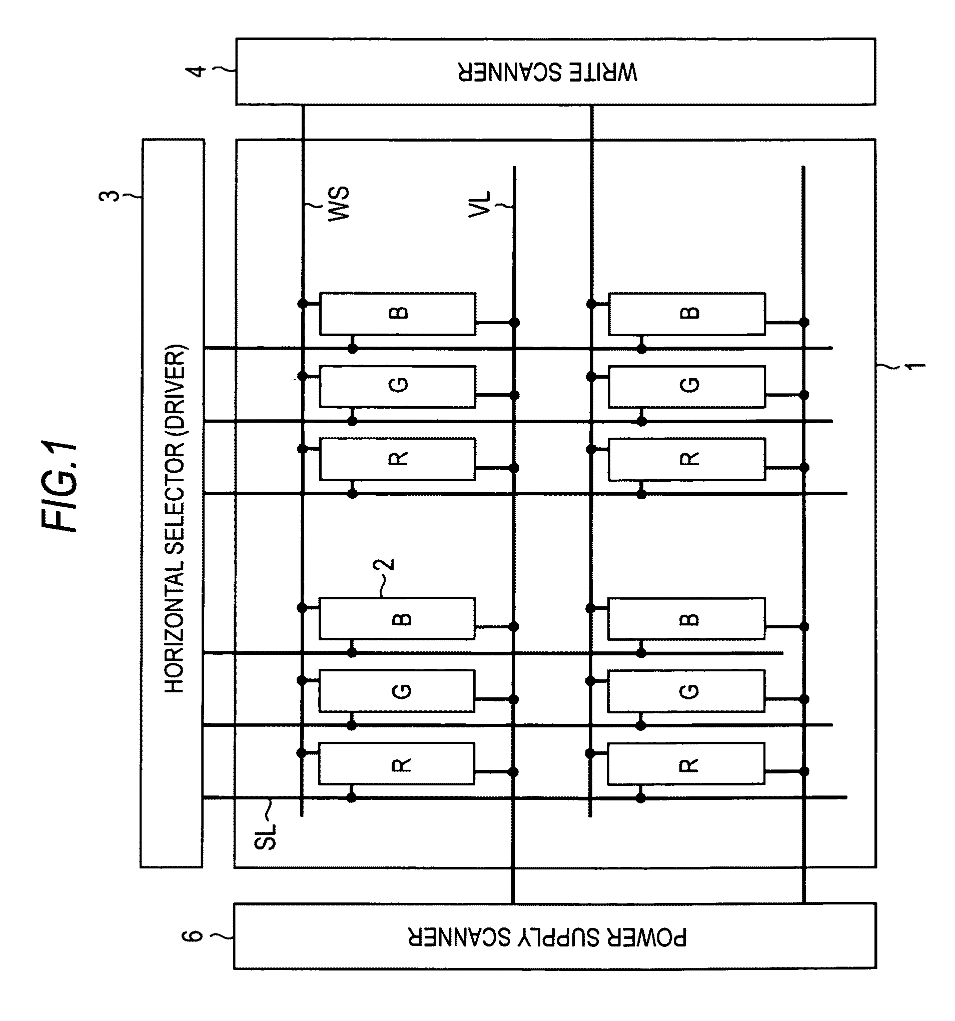
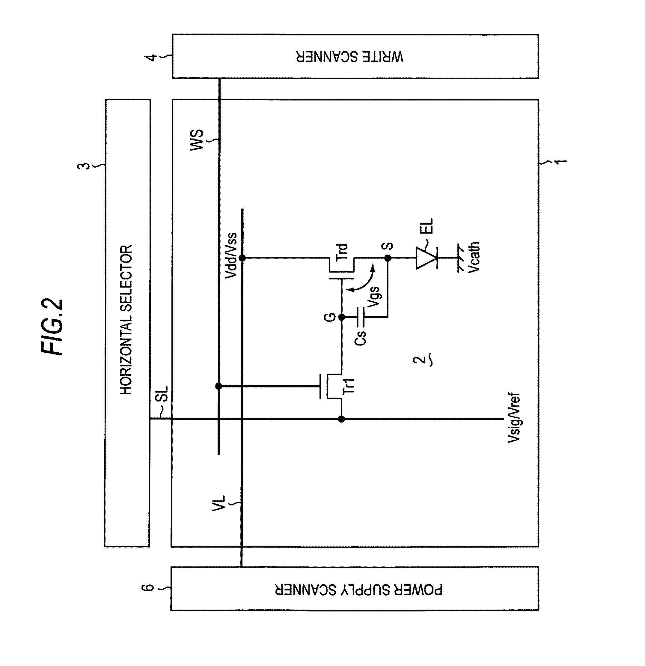
[0103]FIG. 14 is a block diagram showing a panel configuration of a display device according to a third embodiment of the invention. In order to make understanding easier, the codes which are the same as the panel block diagram of the first embodiment shown in FIG. 1 are applied. The display device basically includes a pixel array unit (screen unit) 1 and a drive unit which drives the pixel array unit 1. The pixel array unit 1 includes rows of first scanning lines WS, similarly, rows of second scanning lines DS, columns of signal lines SL, and matrix-state pixels 2 arranged at portions where respective first scanning lines WS and respective signal lines SL intersect. On the other hand, the drive unit includes a write scanner 4, a drive scanner 5 and a horizontal selector 3. The write scanner 4 performs line-sequential scanning of pixels 2 row by row by outputting a control signal to respective first scanning line WS. The drive scanner 5 also performs ling-sequen...


PUM


Abstract

A display device includes: a screen unit; a drive unit; and a signal processing unit, and wherein the screen unit includes rows of scanning lines, columns of signal lines, matrix-state pixel circuits and a light sensor, the drive unit includes a scanner supplying a control signal to the scanning lines and a driver supplying a video signal to the signal lines, the screen unit is sectioned into plural regions each having plural pixel circuits, the drive unit allows plural pixel circuits belonging to different regions to simultaneously emit light, the pixel circuit emits light in accordance with the video signal, the light sensor outputs a luminance signal in accordance with the light emission and the signal processing unit corrects the video signal in accordance with the luminance signal and supplies the signal to the driver.

Description

BACKGROUND OF THE INVENTION[0001]1. Field of the Invention[0002]The present invention relates to a display device displaying images by current-driving a light emitting element arranged at each pixel. The invention also relates to an electronic product using the display device. Particularly, the invention relates to a drive system of a so-called active matrix display device, which controls a current amount flowing in the light emitting element such as an organic EL element by an insulated-gate field effect transistor provided in each pixel circuit or the like.[0003]2. Description of the Related Art[0004]In display devices, for example, in a liquid crystal display, a large number of pixels are arranged in a matrix state and images are displayed by controlling transmission intensity or reflection intensity of incident light in each pixel in accordance with image information to be displayed. This is the same as in an organic EL display in which organic EL elements are used for pixels, h...

Claims


Application Information

Patent Timeline
Patent Type & Authority Patents(United States)
IPC IPC(8): G06F3/038G09G3/30G09G5/00
CPCG09G3/3233G09G2300/0417G09G2300/0819G09G2300/0842G09G2300/0861G09G2310/0262G09G2320/0233G09G2320/043G09G2360/145H01L27/3269H10K59/13H01L22/10
Inventor YAMASHITA, JUNICHIUCHINO, KATSUHIDE
Owner JOLED INC
Why Eureka
Try Eureka