Display device and electronic product

a technology of electronic products and display devices, applied in static indicating devices, solid-state devices, instruments, etc., can solve the problems of image quality failure called “burning” and the luminance of the pixel in the organic el display deteriorating with time, and achieve the effect of compensating the luminance deterioration of pixels

Active Publication Date: 2012-07-03
JOLED INC
View PDF14 Cites 0 Cited by
  • Summary
  • Abstract
  • Description
  • Claims
  • Application Information

AI Technical Summary

Benefits of technology

[0016]It is preferable that the signal processing unit supplies a video signal for display during a display period in which video is displayed in the screen unit, and supplies a video signal for detection during a detection period in which video is not displayed in the screen unit. The signal processing unit supplies the video signal for detection in each frame and allows only pixel circuits of detection targets to emit light. The signal processing unit compares a first luminance signal outputted from the light sensor during a first period with a second luminance signal outputted from the light sensor during a second period after the first period, corrects a video signal in accordance with the comparison result and supplies the signal to the driver. The light sensor outputs the luminance signal in a time-division manner over plural detection periods. The amount of light received by the light sensor in the detection period is higher than the amount of light received by the light sensor in the display period. The signal processing unit makes a level of the video signal for detection higher than the maximum level of the video signal for display. The drive unit adjusts a rate of a light emitting period in which the pixel circuit emits light in one frame to allow the rate of the light emitting period in the detection period to be higher than the rate of the light emitting period in the display period.
[0017]According to the embodiment of the invention, the signal processing unit corrects the video signal in accordance with the luminance signal outputted from the light sensor as well as supplies the corrected video signal to the driver of the drive unit. According to the configuration, it is possible to compensate luminance deterioration of pixels by the correction of the video signal, as a result, image quality failures such as “burn-in” which have been problems from the past can be prevented.

Problems solved by technology

In the light emitting element, current / luminance characteristics tend to deteriorate with time.
Accordingly, there is a problem that luminance of the pixel in the organic EL display is reduced with lapse of time.
When the cumulative light emitting time differs in respective pixels in the screen, luminance nonuniformity may occur and an image quality failure called “burn-in” is liable to occur.

Method used


Image

  • Display device and electronic product
  • Display device and electronic product
  • Display device and electronic product

Examples


second embodiment

[Whole Configuration of a Display Device]

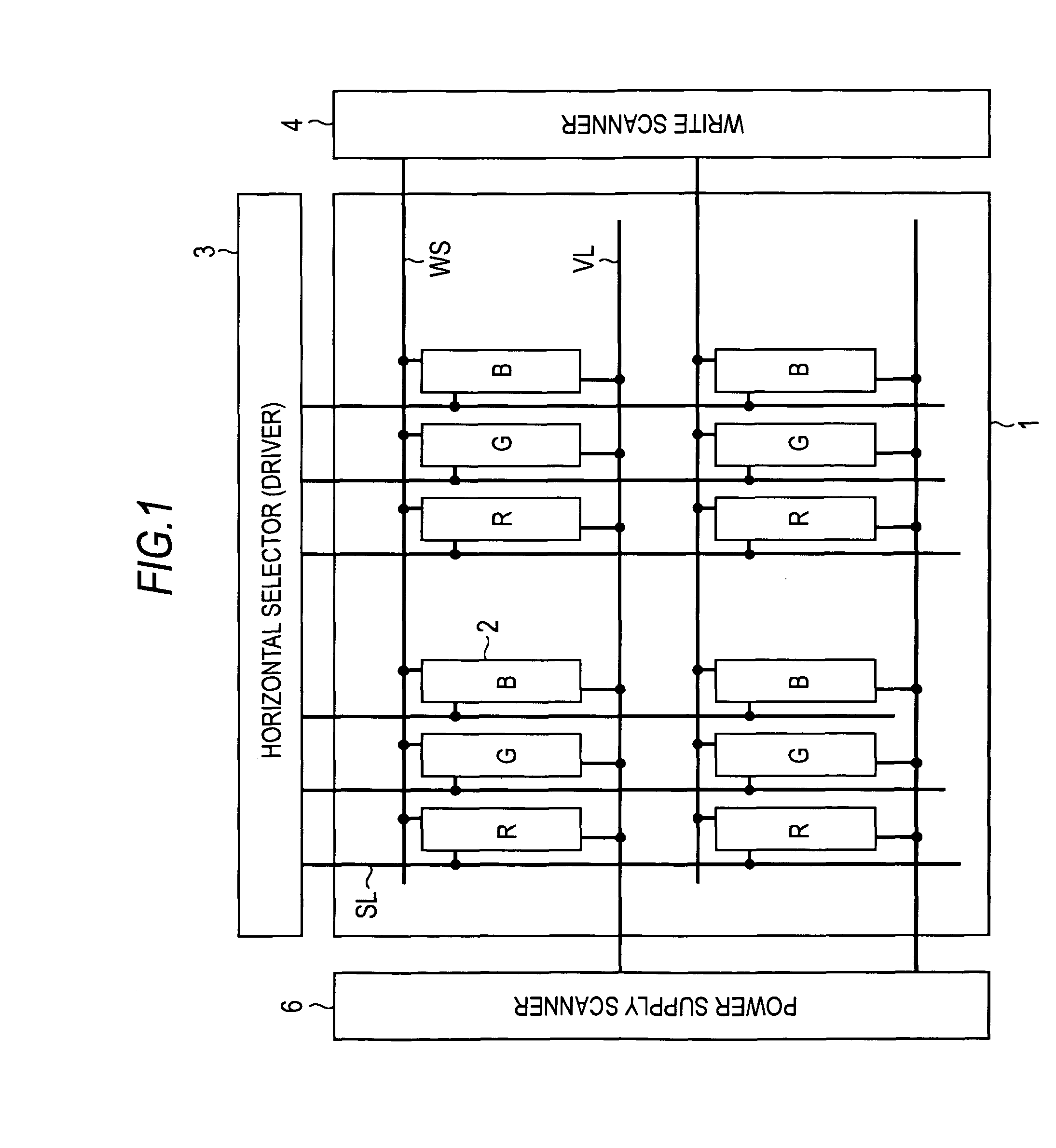
[0090]FIG. 9 is a schematic block diagram showing the whole configuration of a display device according to a second embodiment of the invention. As shown in the drawing, the display device basically includes a screen unit 1, a drive unit and a signal processing unit 10. The screen unit (pixel array unit) 1 has a panel “0” including rows of scanning lines, columns of signal lines and matrix-state pixels arranged at portions where respective scanning lines and respective signal lines intersect and a light sensor 8. The drive unit includes a scanner sequentially supplying a control signal to respective scanning lines and a driver supplying a video signal to respective signal lines. The scanner and the driver are mounted on the panel “0” so as to surround the screen unit 1.

[0091]Each pixel included in the screen unit 1 takes a video signal from a corresponding signal line as well as emits light in accordance with the taken video signal when the p...

third embodiment

[Timing Chart 1]

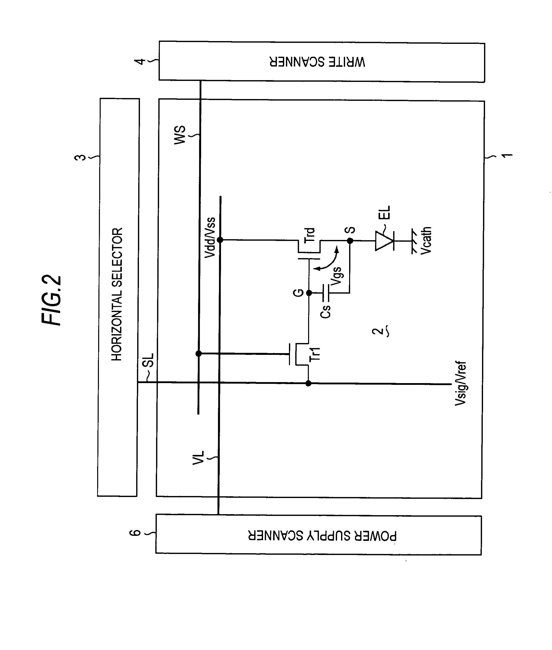
[0096]FIG. 11 is a timing chart for explaining operations of a display device according to a third embodiment of the invention. In the drawing, a potential change of the scanning line WS, a potential change of the feeding line VL and a potential change of the signal line SL are represented in a time axis common to these lines. Additionally, potential changes of the gate G and the source S of the drive transistor are also represented in parallel to these potential changes. The timing chart is basically the same as the timing chart of the first embodiment shown in FIG. 3. The present timing chart represents operations in the display period in which video is displayed in the screen unit. In the display period, a normal video signal is supplied.

[0097]A control signal pulse for turning on the sampling transistor Tr1 is applied to the scanning line WS. The control signal pulse is applied to the scanning line WS in one frame (1f) period so as to correspond to ling-sequentia...

fourth embodiment

[Operation Sequence]

[0107]FIG. 13 shows an operation sequence of a display device according to a fourth embodiment of the invention. The signal processing unit supplies a normal video signal in the display period in which video is displayed in the screen unit and a video signal for luminance detection is supplied in the detection period included in the non-display period in which video is not displayed. The light sensor performs detection of light emitting luminance in the time division manner over plural non-display periods for detecting light emitting luminance of all pixels included in the display unit and outputting luminance signals. In the shown example, the screen is divided into six from an area 1 to an area 6. In the first non-display period, the detection of light emitting luminance of pixels belonging to the areas 1 and 4 is performed. In the next non-display period, the detection of light emitting luminance of pixels belonging to areas 2 and 5 is performed. In the furthe...


PUM


Abstract

A display device includes: a screen unit; a drive unit; and a signal processing unit, wherein the screen unit includes rows of scanning lines, columns of signal lines, matrix-state pixel circuits and a light sensor, the drive unit includes a scanner supplying a control signal to the scanning lines and a driver supplying a video signal to the signal lines, the pixel circuit emits light in accordance with the video signal, the light sensor outputs a luminance signal in accordance with the light emission, and the signal processing unit corrects the video signal in accordance with the luminance signal and supplies the signal to the driver.

Description

BACKGROUND OF THE INVENTION[0001]1. Field of the Invention[0002]The present invention relates to a display device displaying images by current driving a light emitting element arranged at each pixel. The invention also relates to an electronic product using the display device. Particularly, the invention relates to a drive system of a so-called active matrix display device, which controls a current amount flowing in the light emitting element such as an organic EL element by an insulated-gate field effect transistor provided in each pixel circuit.[0003]2. Description of the Related Art[0004]In display devices, for example, in a liquid crystal display, a large number of pixels are arranged in a matrix state and images are displayed by controlling transmission intensity or reflection intensity of incident light in each pixel in accordance with image information to be displayed. This is the same as in an organic EL display in which organic EL elements are used for pixels, however, the ...

Claims


Application Information

Patent Timeline
Patent Type & Authority Patents(United States)
IPC IPC(8): G06F3/038G09G3/20G09G3/30H01L51/50
CPCG09G3/3233G09G2300/043G09G2300/0814G09G2300/0819G09G2320/043G09G2320/046
Inventor YAMASHITA, JUNICHIUCHINO, KATSUHIDE
Owner JOLED INC
Why Eureka
Try Eureka