Display device and electronic product

a technology of electronic products and display devices, applied in the field of display devices, can solve the problems of image quality failure called “burning” prone to occur, the luminance of each pixel in the organic el display is deteriorated with time, and the luminance of the organic el display is reduced with lapse of time, so as to compensate the luminance deterioration of pixels, reduce the number of light sensors, and improve the effect of image quality

Active Publication Date: 2010-05-13
JOLED INC
View PDF9 Cites 11 Cited by
  • Summary
  • Abstract
  • Description
  • Claims
  • Application Information

AI Technical Summary

Benefits of technology

[0017]According to the embodiment of the invention, the signal processing unit corrects the video signal in accordance with the luminance signal outputted from the light sensor as well as supplies the corrected video signal to the driver of the drive unit. According to the configuration, it is possible to compensate luminance deterioration of pixels by the correction of the video signal, and as a result, image quality failures such as “burn-in” which have been problems from the past can be prevented.
[0018]Particularly, in the embodiment of the invention, the light sensor detects light emitting luminance of each pixel and outputs a corresponding luminance signal. Since the light emitting luminance is detected with respect to each individual pixel, partial luminance nonuniformity can be corrected by correcting the video signal in each pixel even when partial nonuniformity occurs in the screen. In the embodiment of the invention, the screen unit is sectioned and the light sensor is arranged with respect to each section. Each section includes a number of pixels in a range in which the corresponding light sensor can detect light emitting luminance. According to the embodiment of the invention, it is not necessary to provide light sensors so as to correspond to respective pixels for detecting light emitting luminance of each pixel, therefore, the necessary number of light sensors can be drastically reduced, and as a result, it is possible to simplify a display panel structure as well as to reduce costs for the display panel.

Problems solved by technology

In the light emitting element, current / luminance characteristics tend to deteriorate with time.
Accordingly, there is a problem that luminance of each pixel in the organic EL display is reduced with lapse of time.
When the cumulative light emitting time differs in respective pixels in the screen, luminance nonuniformity may occur and an image quality failure called “burn-in” is liable to occur.

Method used


Image

  • Display device and electronic product
  • Display device and electronic product
  • Display device and electronic product

Examples


first embodiment

[Whole Configuration of a Panel]

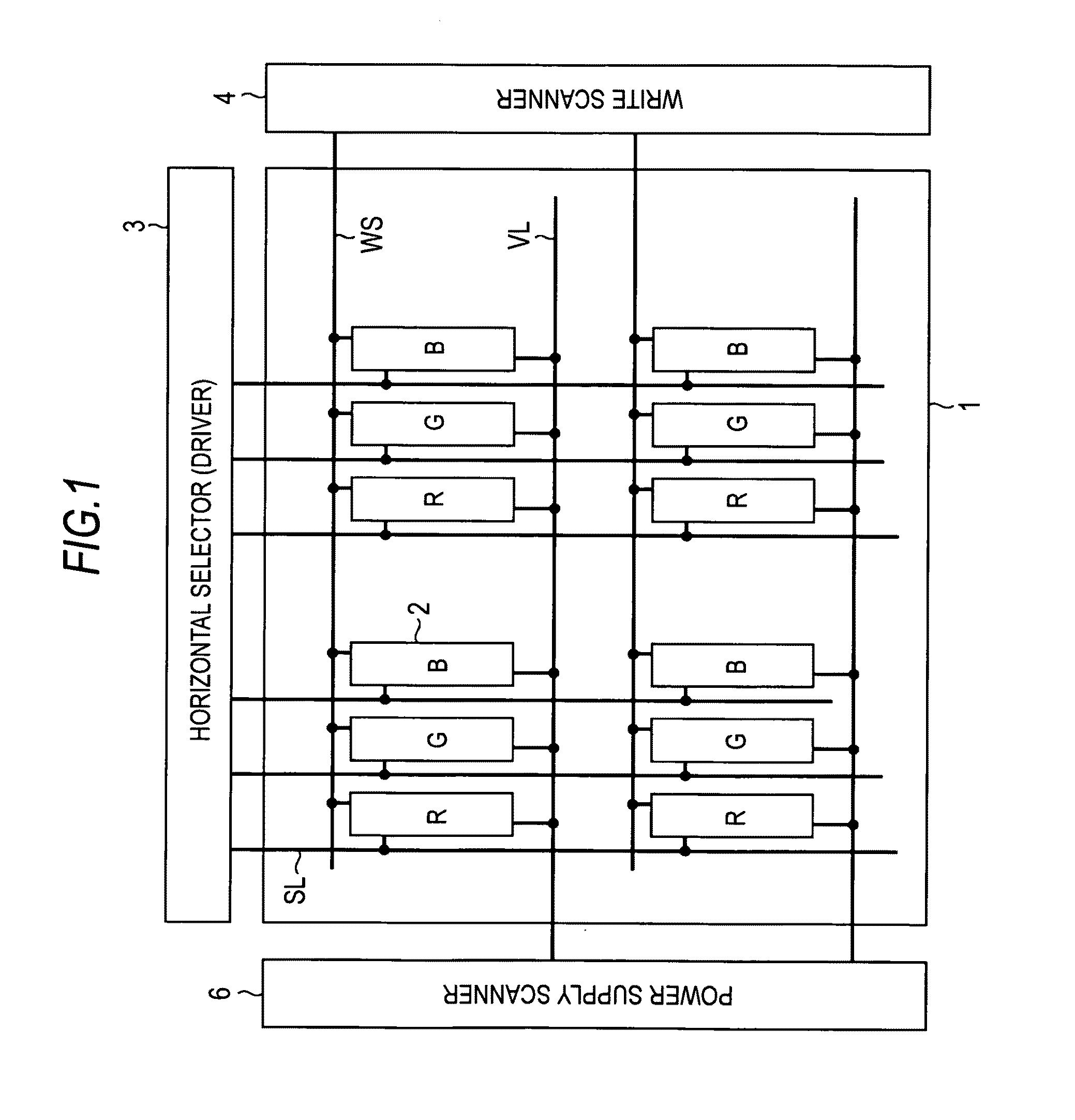
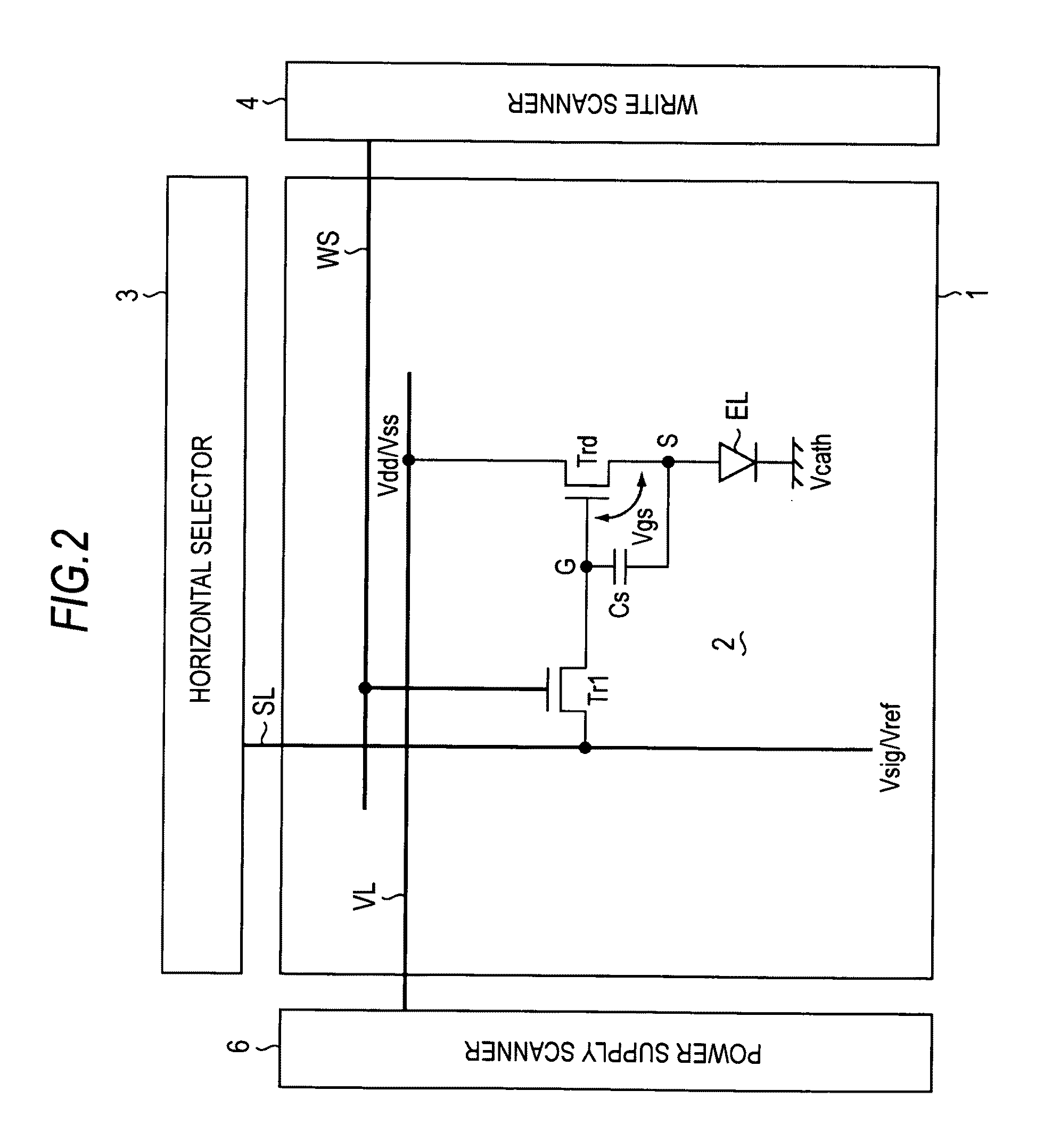
[0058]FIG. 1 is the whole configuration diagram showing a panel which is a main unit of a display device according to an embodiment of the invention. As shown in the drawing, the display device includes a pixel array unit 1 (screen unit) and a drive unit which drives the pixel array unit 1. The pixel array unit 1 has rows of scanning lines WS, columns of signal lines SL, matrix-state pixels 2 arranged at portions where the both lines intersect and feeding lines (power lines) VL arranged so as to correspond to respective lines of respective pixels 2. In the example, any of RGB three primary colors is assigned to each pixel 2 to realize color display. However, the invention is not limited to this and also includes a single-color display device. The drive unit includes a write scanner 4 performing line-sequential scanning of the pixels 2 row by row by sequentially supplying a control signal to respective scanning lines WS, a power supply scanner 6 supply...

modification example

[Modification Example]

[0081]FIG. 6 is a block diagram showing a modification example of the display device according to the first embodiment shown in FIG. 5. In order to make understanding easier, corresponding reference numerals are given to portions corresponding to components shown in FIG. 5. A different point is that the light sensor 8 is arranged on the surface side, not on the reverse side of the panel “0”. When the light sensor 8 is arranged on the surface side, there is an advantage that the light receiving amount is increased as compared with the case of the reverse side. However, when the light sensor 8 is arranged on the surface side of the panel “0”, there occurs a disadvantage that light emission from part of pixels is sacrificed.

[Configuration of the Panel]

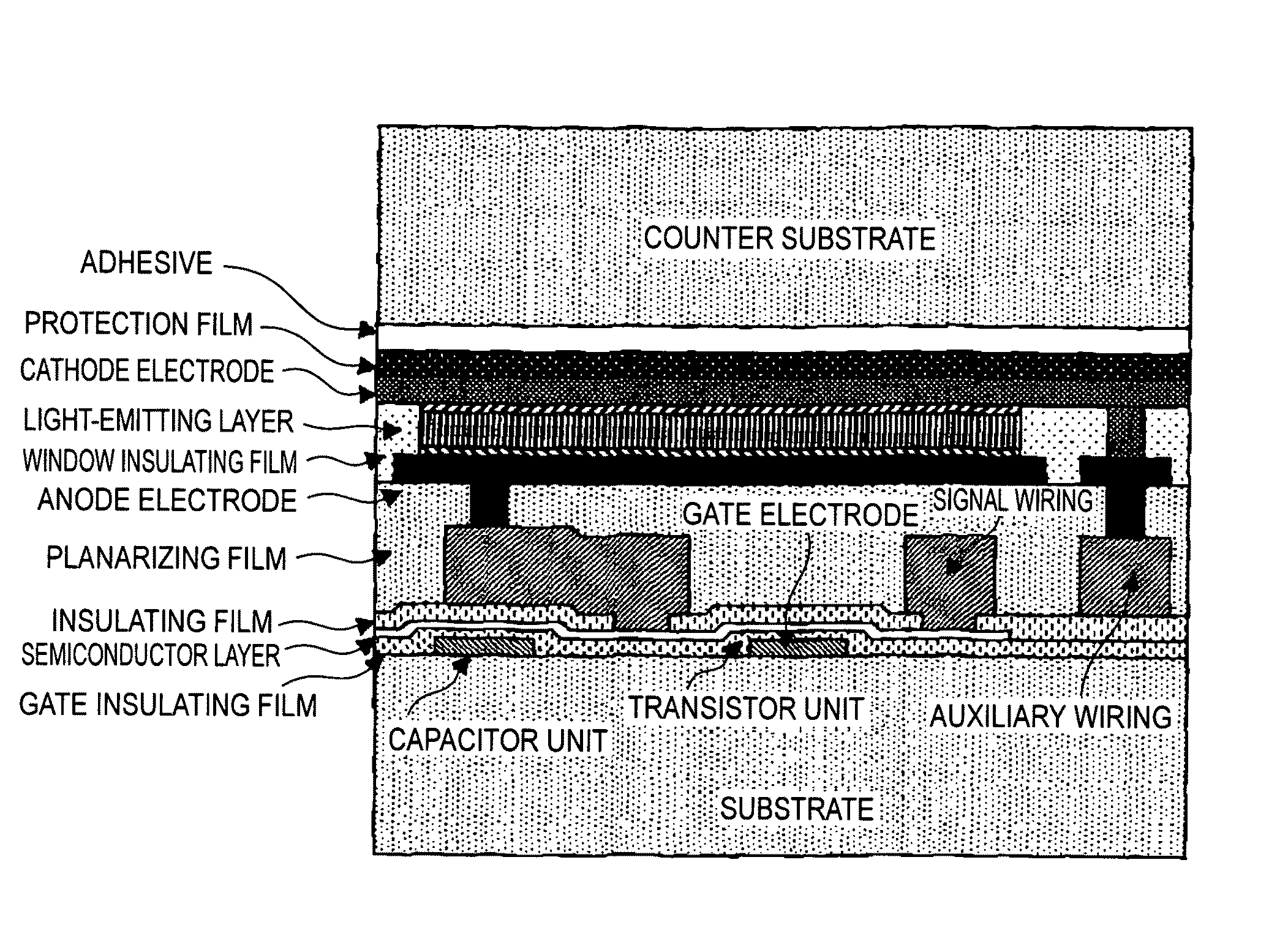
[0082]FIG. 7 is a schematic plan view and a cross-sectional view showing a configuration of the panel included in the display device shown in FIG. 5. As shown in the drawing, the screen unit (pixel array unit) 1 is a...

second embodiment

[Dynamic Range of Luminance Signals]

[0099]FIG. 13 is a graph showing the dynamic range of luminance signals outputted from the light sensor. A horizontal axis is for the distance from the central position of the light sensor and a vertical axis is for the output voltage of the luminance signal. The distance in the horizontal axis is represented by the number of pixels from the light sensor. As shown in the drawing, the value of light received by the light sensor is reduced as the distance from the light sensor becomes long even when the pixel luminance is the same. In the shown example, the output level of the luminance signal of the pixel at the central position reaches 3V, while the output voltage of the luminance signal of the pixel apart from the central position by 20 pixels in the number of pixels is reduced to 0.3V, which is approximately 1 / 10. In the burn-in correction system shown in FIG. 5, the output from the light sensor 8 is amplified, and then, the analog signal is con...


PUM


Abstract

A display device includes: a screen unit; a drive unit; and a signal processing unit, wherein the screen unit includes rows of scanning lines, columns of signal lines, matrix-state pixel circuits and a light sensor, the drive unit includes a scanner supplying a control signal to the scanning lines and a driver supplying a video signal to the signal lines, the screen unit is sectioned into plural regions each having plural pixel circuits, the pixel circuit emits light in accordance with the video signal, the light sensor is arranged with respect to each region and outputs a luminance signal in accordance with the light emission; and the signal processing unit corrects the video signal in accordance with the luminance signal and supplies the signal to the driver.

Description

BACKGROUND OF THE INVENTION[0001]1. Field of the Invention[0002]The present invention relates to a display device displaying images by current-driving a light emitting element arranged at each pixel. The invention also relates to an electronic product using the display device. Particularly, the invention relates to a drive system of a so-called active matrix display device, which controls a current amount flowing in the light emitting element such as an organic EL element by an insulated-gate field effect transistor provided in each pixel circuit.[0003]2. Description of the Related Art[0004]In display devices, for example, in a liquid crystal display, a large number of pixels are arranged in a matrix state and images are displayed by controlling transmission intensity or reflection intensity of incident light in each pixel in accordance with image information to be displayed. This is the same as in an organic EL display in which organic EL elements are used for pixels, however, the ...

Claims


Application Information

Patent Timeline
Patent Type & Authority Applications(United States)
IPC IPC(8): G09G3/20G09G5/00
CPCG09G3/3233G09G2300/043G09G2300/0852G09G3/3225G09G2320/046G09G2360/145G09G2320/043
Inventor YAMASHITA, JUNICHIOMOTO, KEISUKEUCHINO, KATSUHIDE
Owner JOLED INC
Why Eureka
Try Eureka