Display device and electronic product having light sensors in plural pixel regions

a technology of electronic products and display devices, which is applied in the field of display devices, can solve the problems of image quality failure called “burning” and the luminance of each pixel in the organic el display, and achieve the effects of simplifying the structure reducing the cost of the display panel, and reducing the number of light sensors

Inactive Publication Date: 2014-08-21
JOLED INC
View PDF3 Cites 0 Cited by
  • Summary
  • Abstract
  • Description
  • Claims
  • Application Information

AI Technical Summary

Benefits of technology

[0018]According to the embodiment of the invention, the signal processing unit corrects the video signal in accordance with the luminance signal outputted from the light sensor as well as supplies the corrected video signal to the driver of the drive unit. According to the configuration, it is possible to compensate luminance deterioration of pixels by the correction of the video signal, as a result, image quality failures such as “burn-in” which have been problems from the past can be prevented.
[0020]Particularly, in the embodiment of the invention, the screen unit is sectioned and the light sensor is arranged with respect to each section. Each section includes a number of pixels in a range in which the corresponding light sensor can detect light emitting luminance. According to the embodiment of the invention, it is not necessary to provide light sensors so as to correspond to respective pixels for detecting light emitting luminance of each pixel, therefore, the necessary number of light sensors can be drastically reduced, as a result, it is possible to simplify a display panel structure as well as to reduce costs for the display panel.
[0021]Furthermore, in a display device according to an embodiment, a selector is arranged between the panel and the signal processing unit (for example, a DSP). The selector supplies luminance signals outputted from plural light sensors arranged so as to correspond to plural regions by switching the signals. It is possible to reduce the number of wirings connecting between plural light sensors and the signal processing unit by interposing the selector. When the signal processing unit includes an IC chip (for example, a FPGA or an ASIC), the number of pins for connecting to the plural light sensors can be reduced. Accordingly, a general-purpose IC chip can be used even when the number of light sensors exceeds the number of pins of the DSP.
[0022]Further, according to the embodiment of the invention, plural light sensors are grouped into blocks by a given number of sensors. The signal processing unit receives luminance signals by each block, and performs correction processing of the video signal based on the luminance signals. In order to process analog luminance signals outputted from the light sensors in the signal processing unit (for example, the DSP), an amplifier for amplifying analog luminance signals or a converter converting analog data of amplified luminance signals into digital data are necessary. According to the embodiment of the invention, the light sensors are grouped into blocks by a given number of sensors, thereby using the amplifier and converter in common by the light sensors which are grouped into blocks, which realizes reduction of the number of components.

Problems solved by technology

In the light emitting element, current / luminance characteristics tend to deteriorate with time.
Accordingly, there is a problem that luminance of each pixel in the organic EL display is reduced with lapse of time.
When the cumulative light emitting time differs in respective pixels in the screen, luminance nonuniformity may occur and an image quality failure called “burn-in” is liable to occur.

Method used


Image

  • Display device and electronic product having light sensors in plural pixel regions
  • Display device and electronic product having light sensors in plural pixel regions
  • Display device and electronic product having light sensors in plural pixel regions

Examples


first embodiment

Whole Configuration of a Panel

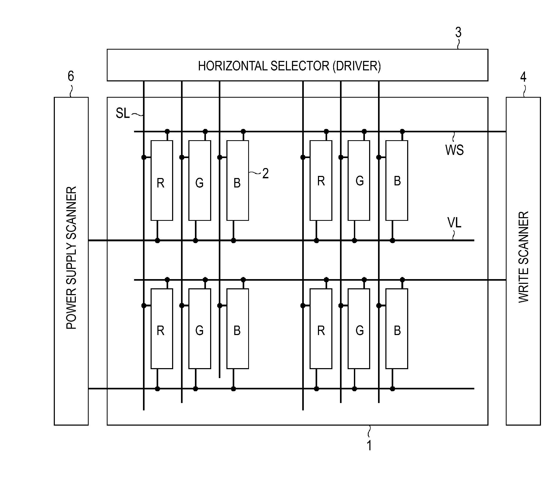
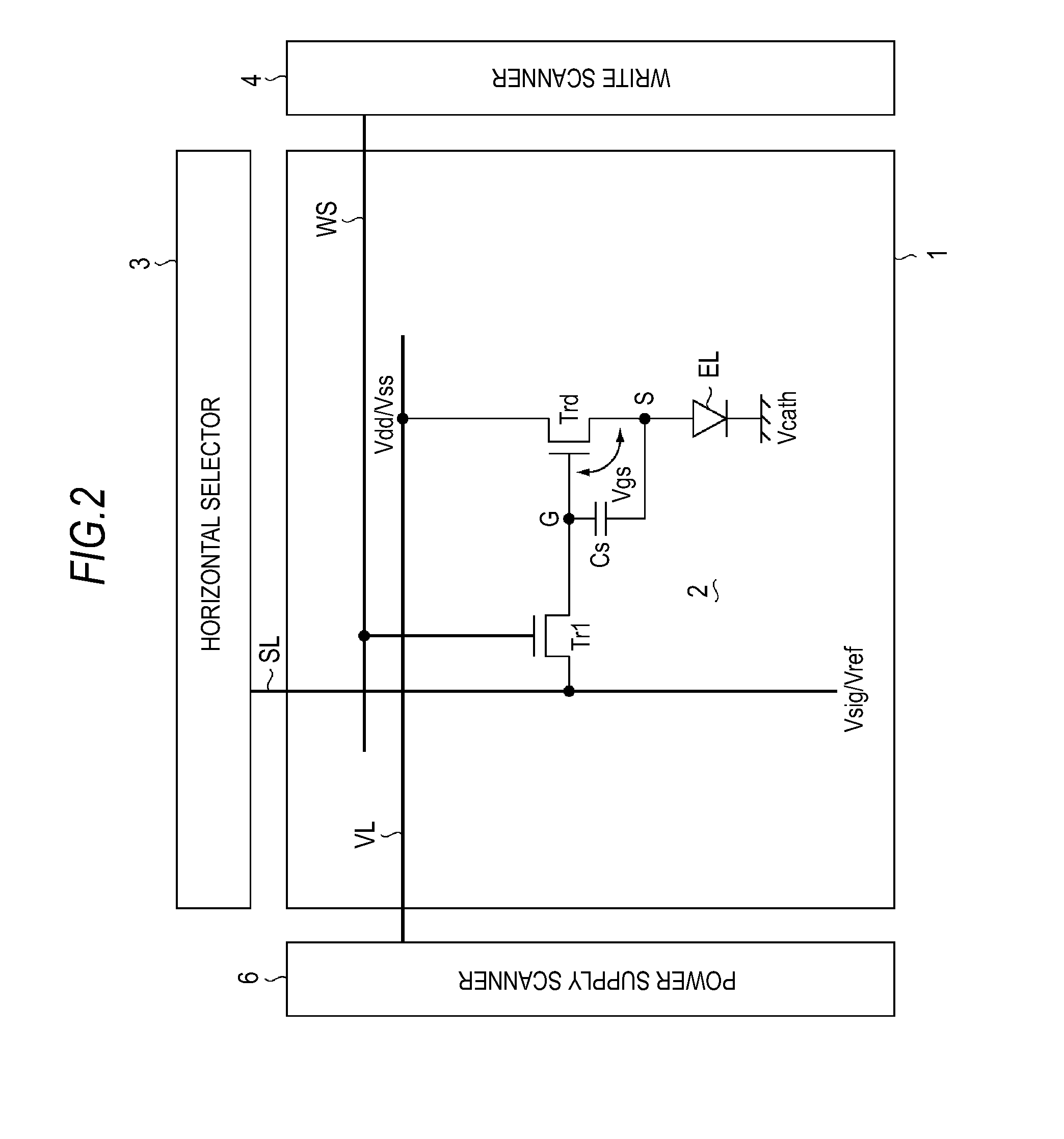
[0067]FIG. 1 is the whole configuration diagram showing a panel which is a main unit of a display device according to the embodiment of the invention. As shown in the drawing, the display device includes a pixel array unit 1 (screen unit) and a drive unit which drives the pixel array unit 1. The pixel array unit 1 has rows of scanning lines WS, columns of signal lines SL, matrix-state pixels 2 arranged at portions where the both lines intersect and feeding lines (power lines) VL arranged so as to correspond to respective lines of respective pixels 2. In the example, any of RGB three primary colors is assigned to each pixel 2 to realize color display. However, the invention is not limited to this and also includes a single-color display device. The drive unit includes a write scanner 4 performing line-sequential scanning of the pixels 2 row by row by sequentially supplying a control signal to respective scanning lines WS, a power supply scanner 6 supplyi...

modification example

[0090]FIG. 6 is a block diagram showing a modification example of the display device according to the first embodiment shown in FIG. 5. In order to make understanding easier, corresponding reference numerals are given to portions corresponding to components shown in FIG. 5. A different point is that the light sensor 8 is arranged on the surface side, not on the reverse side of the panel “0”. When the light sensor 8 is arranged on the surface side, there is an advantage that the light receiving amount is increased as compared with the case of the reverse side. However, when the light sensor 8 is arranged on the surface side of the panel “0”, there occurs a disadvantage that light emission from part of pixels is sacrificed.

[Configuration of the Panel]

[0091]FIG. 7 is a schematic plan view and a cross-sectional view showing a configuration of the panel included in the display device shown in FIG. 5. As shown in the drawing, the screen unit (pixel array unit) 1 is arranged at the center ...

second embodiment

Configuration

[0124]FIG. 16 is a schematic block diagram showing a second embodiment. A display device according to the second embodiment basically includes a screen unit, a drive unit and a signal processing unit (DSP) 10. The screen unit (not shown) has a panel including rows of scanning lines, columns of signal lines, matrix-state pixels arranged at portions where respective scanning lines and respective signal lines intersect and a light sensor. The drive unit (not shown) includes a scanner sequentially supplying a control signal to respective scanning lines and a driver supplying a video signal to respective signal lines. The pixel (not shown) takes a video signal from the signal line as well as emits light in accordance with the taken video signal when selected in accordance with the control signal supplied from the scanning line. The light sensor detects light emitting luminance of each pixel and outputs a corresponding luminance signal. The signal processing unit 10 corrects ...


PUM


Abstract

A display device includes: a screen unit; a drive unit; a signal processing unit; and a selector, wherein the screen unit includes rows of scanning lines, columns of signal lines, matrix-state pixel circuits and a light sensor, the drive unit includes a scanner supplying a control signal to the scanning lines and a driver supplying a video signal to the signal lines, the screen unit is sectioned into plural regions each having plural pixel circuits, the pixel circuit emits light in accordance with the video signal, the light sensor is arranged with respect to each region and outputs a luminance signal in accordance with the light emission, the selector supplies plural luminance signals to the signal processing unit by switching the signals, and the signal processing unit corrects the video signal in accordance with the luminance signals and supplies the video signal to the driver.

Description

CROSS REFERENCES TO RELATED APPLICATIONS[0001]The present application is a continuation of application Ser. No. 12 / 588,520, filed Oct. 19, 2009, which in turn claims priority from Japanese Application No.: 2008-286781, filed in the Japan Patent Office on Nov. 7, 2008, the entirety of which being incorporated herein by reference.BACKGROUND OF THE INVENTION[0002]1. Field of the Invention[0003]The present invention relates to a display device displaying images by current-driving a light emitting element arranged at each pixel. The invention also relates to an electronic product using the display device. Particularly, the invention relates to a drive system of a so-called active matrix display device, which controls a current amount flowing in the light emitting element such as an organic EL element by an insulated-gate field effect transistor provided in each pixel circuit.[0004]2. Description of the Related Art[0005]In display devices, for example, in a liquid crystal display, a large...

Claims


Application Information

Patent Timeline
Patent Type & Authority Applications(United States)
IPC IPC(8): G09G3/30H05B44/00
CPCG09G3/30G09G2320/045G09G2320/046G09G2360/145G09G2360/147G09G3/3233
Inventor YAMASHITA, JUNICHIUCHINO, KATSUHIDE
Owner JOLED INC
Why Eureka
Try Eureka