Method for improving device performance using dual stress liner boundary

a technology of dual stress liner and boundary, which is applied in the field of integrated circuit dual stress liner, can solve the problem of not improving the performance of the transistor accordingly

Active Publication Date: 2012-05-17
TEXAS INSTR INC
View PDF2 Cites 16 Cited by
  • Summary
  • Abstract
  • Description
  • Claims
  • Application Information

AI Technical Summary

Benefits of technology

[0007]The following presents a simplified summary in order to provide a basic understanding of one or more aspects of the invention. This summary is not an extensive overview of the invention, and is neither intended to identify key or critic

Problems solved by technology

As technology scales, transistor performance is not improving accordingly.

Method used


Image

  • Method for improving device performance using dual stress liner boundary
  • Method for improving device performance using dual stress liner boundary
  • Method for improving device performance using dual stress liner boundary

Examples


Embodiment Construction

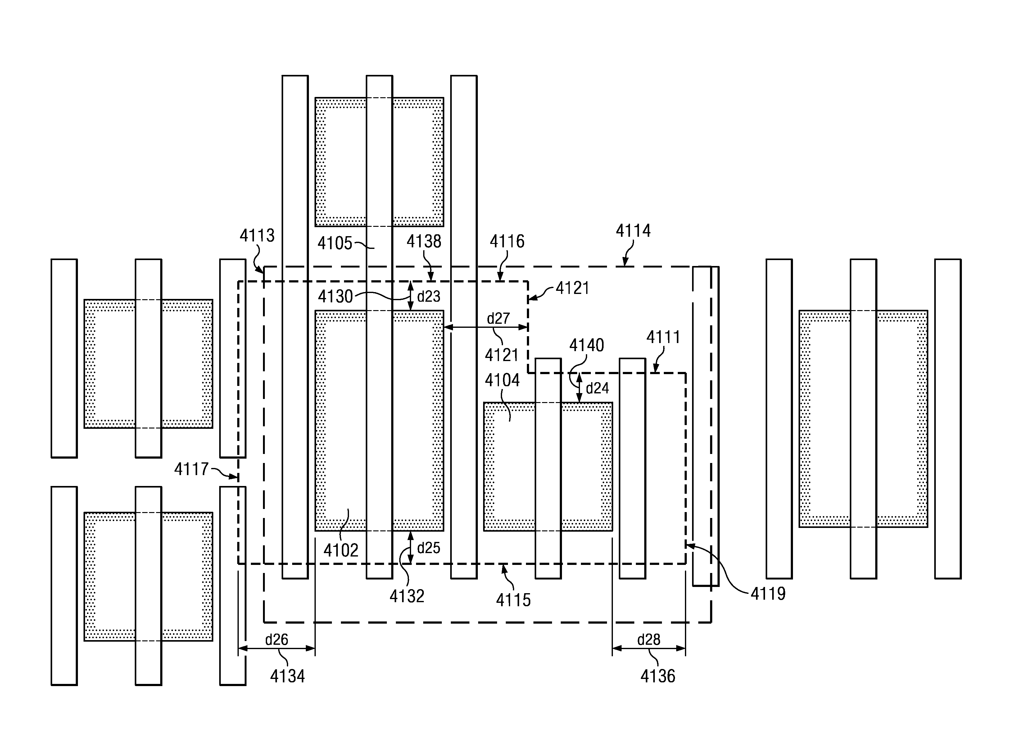
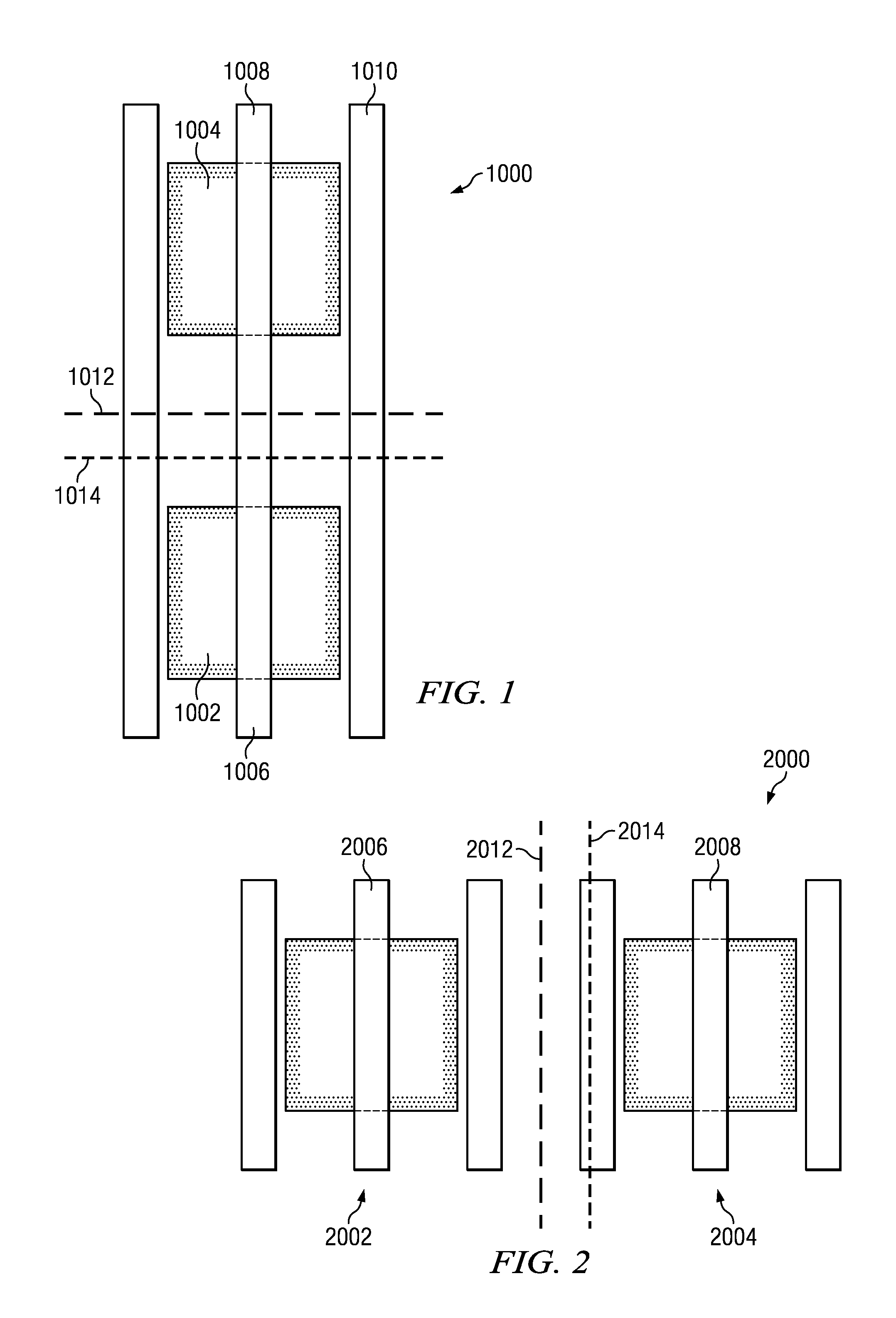
[0012]The present invention is described with reference to the attached figures, wherein like reference numerals are used throughout the figures to designate similar or equivalent elements. The figures are not drawn to scale and they are provided merely to illustrate the invention. Several aspects of the invention are described below with reference to example applications for illustration. It should be understood that numerous specific details, relationships, and methods are set forth to provide an understanding of the invention. One skilled in the relevant art, however, will readily recognize that the invention can be practiced without one or more of the specific details or with other methods. In other instances, well-known structures or operations are not shown in detail to avoid obscuring the invention. The present invention is not limited by the illustrated ordering of acts or events, as some acts may occur in different orders and / or concurrently with other acts or events. Furth...


PUM


Abstract

An integrated circuit with DSL borders perpendicular to the tranistor gates primarily inside the nwell and with DSL borders parallel to the transistor gates primarily outside the nwell. A method for forming an integrated circuit with DSL borders perpendicular to the tranistor gates primarily inside the nwell and with DSL borders parallel to the transistor gates primarily outside the nwell.

Description

[0001]This application claims the benefit of U.S. Provisional Application No. 61 / 409,583, filed Nov. 3, 2010, the entirety of which is herein incorporated by reference.FIELD OF THE INVENTION[0002]This invention relates to the field of integrated circuits. More particularly, this invention relates to dual stress liners in integrated circuitsBACKGROUND OF THE INVENTION[0003]As technology scales, transistor performance is not improving accordingly. In order to increase transistor performance, various processes have been implemented to apply stress to the channel region to enhance carrier mobility. Compressive stress enhances hole mobility when applied parallel to the current flow in a PMOS transistor. One method to apply compressive stress in PMOS transistors is to remove silicon from the source and drain regions and replace it with epitaxially grown silicon germanium (SiGe). Germanium is a larger atom than silicon so the lattice constant of crystalline SiGe is greater than crystalline...

Claims


Application Information

Patent Timeline
IPC IPC(8): H01L27/092H01L21/8238
CPCH01L29/1033H01L27/092H01L27/0203H01L29/0638H01L29/7843H01L21/823807H01L27/0207H01L27/0925
InventorCHOI, YOUN SUNGBALDWIN, GREG CHARLES
OwnerTEXAS INSTR INC