System and apparatus for flowable deposition in semiconductor fabrication

a technology of flowable deposition and semiconductor, applied in mechanical equipment, chucks, manufacturing tools, etc., can solve the problems of increasing difficulty in high aspect ratio (ar) features, void-free filling of narrow width, and budget reduction

Active Publication Date: 2012-06-28
NOVELLUS SYSTEMS
View PDF34 Cites 619 Cited by
  • Summary
  • Abstract
  • Description
  • Claims
  • Application Information

AI Technical Summary

Benefits of technology

[0026]In some further implementations of the semiconductor fabrication module, the wafer support apparatus may further include a guard ring. The guard ring may be supported by the chuck, may be substantially axially symmetric, and may have an inner diameter less than the nominal diameter of the chuck. The guard ring may be offset from the chuck along the chuck center axis by between 15 microns and 250 microns. The offset from the chuck may be provided by posts which are in thermal contact with the chuck across the portion of the overlap not offset from the chuck, and the surfaces of the guard ring and the dielectric break which face each other may be separated by a gap of 0.015″ to 0.050″ and surfaces of the guard ring and the housing which face each other are sep...

Problems solved by technology

As device geometries shrink and thermal budgets are reduced, void-free filling of narrow width, high aspect ra...

Method used


Image

  • System and apparatus for flowable deposition in semiconductor fabrication
  • System and apparatus for flowable deposition in semiconductor fabrication
  • System and apparatus for flowable deposition in semiconductor fabrication

Examples


Embodiment Construction

[0073]Introduction

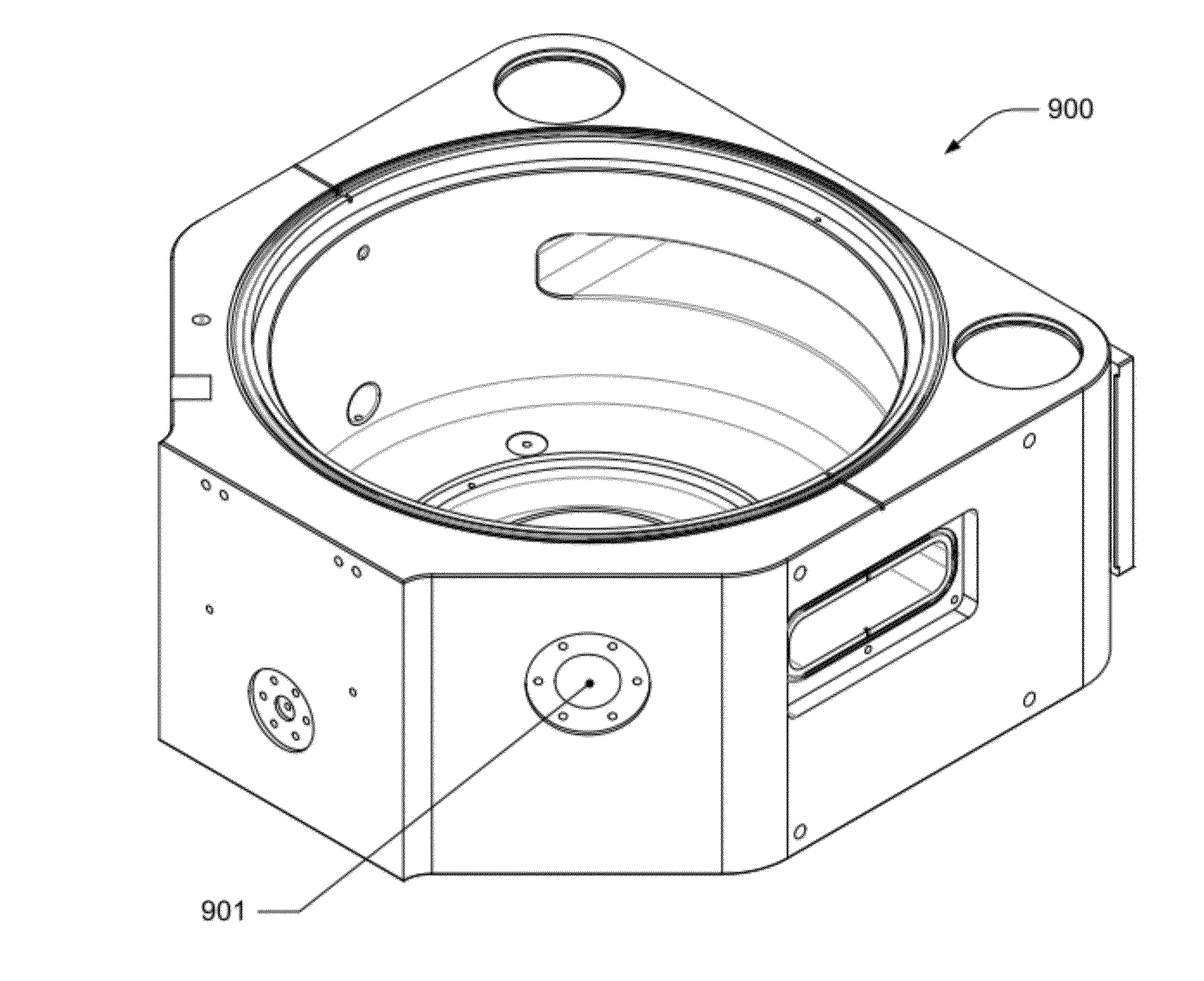
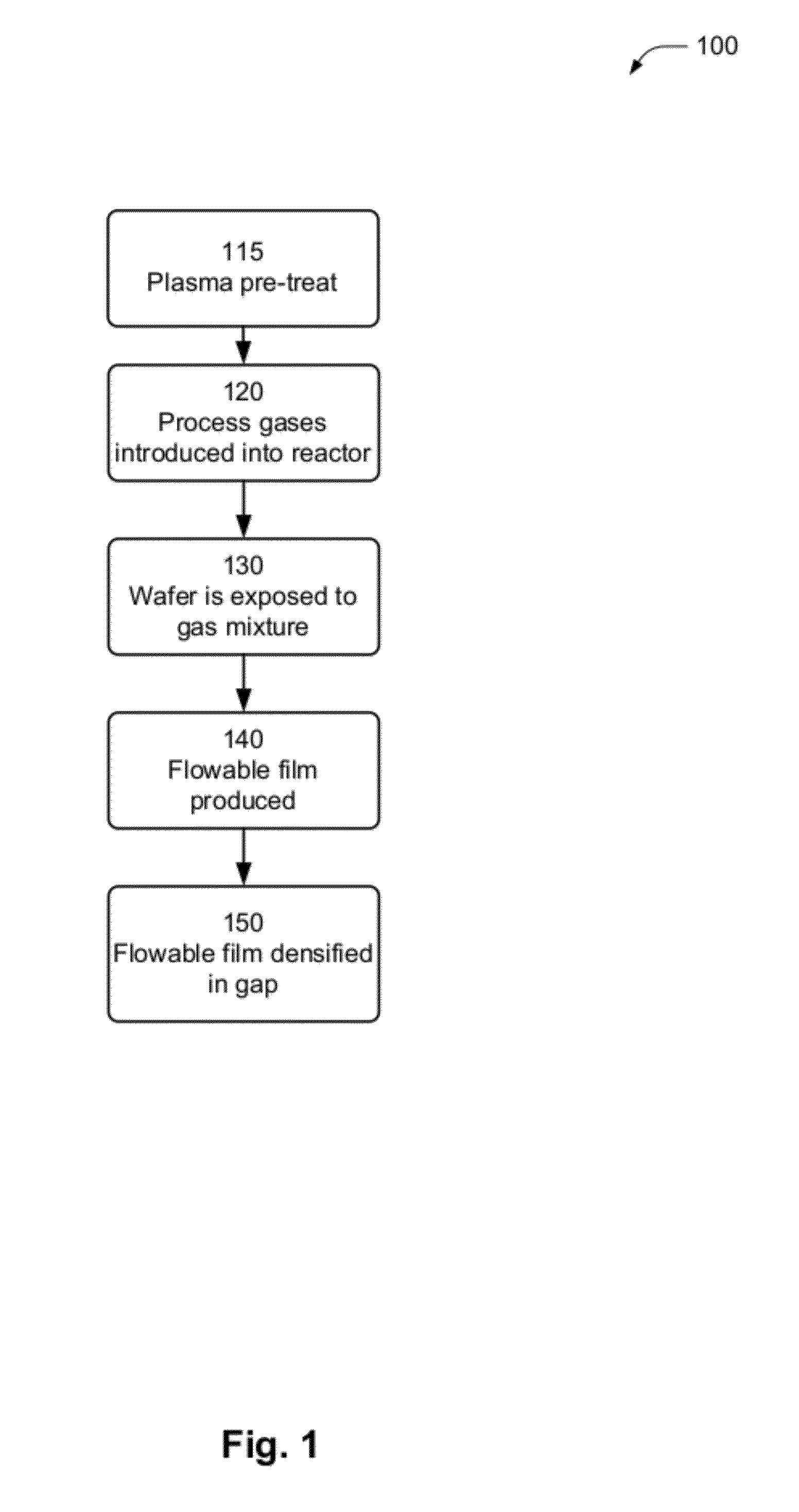
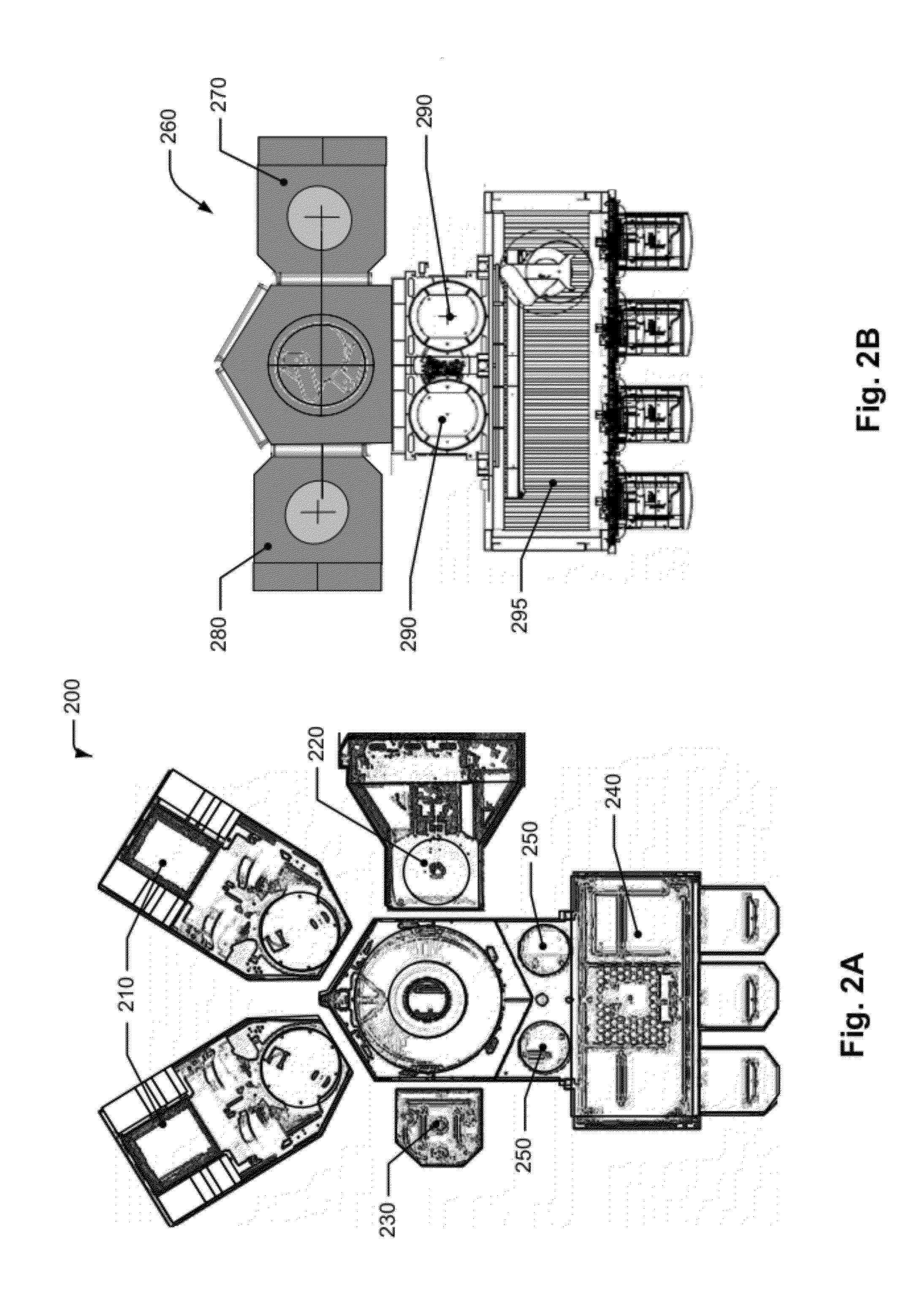
[0074]Provided herein are apparatuses, systems and methods for dielectric gap fill. According to various embodiments, the apparatuses and systems are configured for gap fill in various integration processes that include deposition of a flowable dielectric material, in certain embodiments, a flowable oxide material. While the discussion below includes details of a flowable oxide deposition process, similar techniques and equipment may also be used for flowable nitrides and carbides; the present application should not be read as being limited to flowable oxide techniques and is intended to encompass such additional flowable film techniques as well. These methods, apparatuses, systems, and technologies are also not restricted solely to gap fill applications, however, and may be of use in any flowable deposition semiconductor fabrication process, including, but not limited to, planarization, sacrificial film deposition, and pore sealing. In certain embodiments, the app...


PUM

PropertyMeasurementUnit
Temperatureaaaaaaaaaa

Abstract

Electronic device fabrication processes, apparatuses and systems for flowable gap fill or flowable deposition techniques are described. In some implementations, a semiconductor fabrication chamber is described which is configured to maintain a semiconductor wafer at a temperature near 0° C. while maintaining most other components within the fabrication chamber at temperatures on the order of 5-10° C. or higher than the wafer temperature.

Description

CROSS-REFERENCE TO RELATED APPLICATIONS[0001]This application claims benefit under 35 U.S.C. §119(e) to U.S. Provisional Application No. 61 / 425,150, filed Dec. 20, 2010, which is incorporated by reference herein.BACKGROUND OF THE INVENTION[0002]This invention relates to electronic device fabrication processes, apparatuses and systems. In particular embodiments, it relates to dielectric gap fill processes, apparatuses and systems.[0003]It is often necessary in semiconductor processing to fill high aspect ratio gaps with insulating material. This is the case for shallow trench isolation (STI), inter-metal dielectric (IMD) layers, inter-layer dielectric (ILD) layers, pre-metal dielectric (PMD) layers, passivation layers, etc. As device geometries shrink and thermal budgets are reduced, void-free filling of narrow width, high aspect ratio (AR) features (e.g., AR>6:1) becomes increasingly difficult due to limitations of existing deposition processes.[0004]New methods, apparatuses, sys...

Claims


Application Information

Patent Timeline
IPC IPC(8): B23B31/02
CPCC23C16/401C23C16/45565C23C16/45574C23C16/4585C23C16/4586Y10T279/34H01L21/67109H01L21/6719H01L21/68785H01L21/68792C23C16/463H01L21/02H01L21/205H01L21/683
Inventor MOHN, JONATHAN D.TE NIJENHUIS, HARALDHAMILTON, SHAWN M.MADRIGAL, KEVINLINGAMPALLI, RAMKISHAN RAO
Owner NOVELLUS SYSTEMS
Why Eureka
Try Eureka