Display device

a display device and display technology, applied in the field of display devices, to achieve the effect of increasing the distance with which a viewer can see 3d images by the naked eye, and high-convenient display devices

Inactive Publication Date: 2012-08-16
SEMICON ENERGY LAB CO LTD
View PDF5 Cites 13 Cited by
  • Summary
  • Abstract
  • Description
  • Claims
  • Application Information

AI Technical Summary

Benefits of technology

[0009]In view of the above, an object of one embodiment of the present invention is to increase the range of distance (between a display screen and the eye of a viewer) with which the viewer can see 3D images by the naked eye.
[0013]According to one embodiment of the present invention, the range of distance with which a viewer can see 3D images by the naked eye can be increased. A highly convenient display device can be provided as a result.

Problems solved by technology

However, in order to display 3D images by a parallax barrier method, a specific distance is needed between a display screen and the eye of a viewer.

Method used


Image

  • Display device
  • Display device
  • Display device

Examples


embodiment 1

[0028]First, a display device according to one embodiment of the present invention will be described with reference to FIG. 1, FIGS. 2A and 2B, FIGS. 3A to 3C, and FIGS. 4A and 4B.

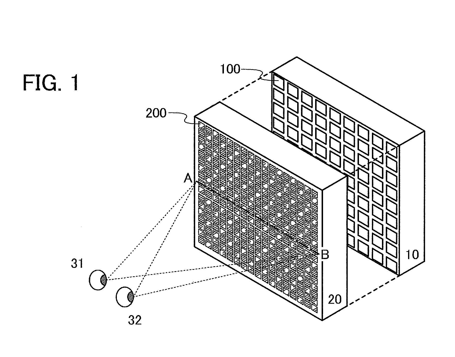
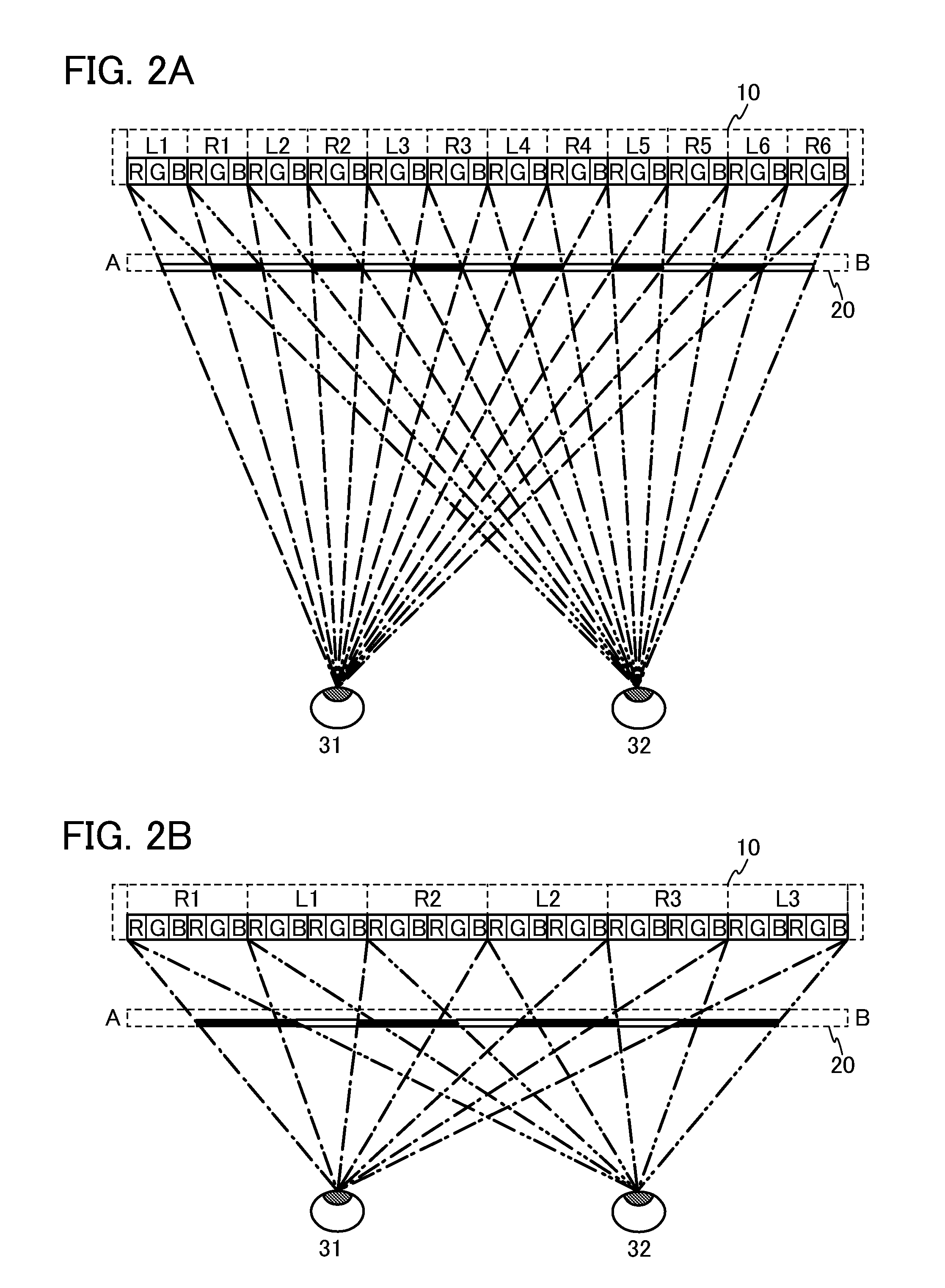
[0029]FIG. 1 is a schematic diagram of a display device according to one embodiment of the present invention. The display device illustrated in FIG. 1 includes a display panel 10 in which a plurality of pixel regions 100 are arranged in matrix, and a shutter panel 20 in which a plurality of optical shutter regions 200 are arranged in matrix. The density of the plurality of optical shutter regions 200 is higher than that of the plurality of pixel regions 100. In other words, the number of the optical shutter regions 200 included in the shutter panel 20 is larger than that of the pixel regions 100 included in the display panel 10. FIG. 1 shows a left eye 31 and a right eye 32 of a viewer in order to show a state of the viewer's perception.

[0030]The shutter panel 20 is provided in the direction of light emiss...

embodiment 2

[0051]In this embodiment, specific examples of a shutter panel in the display device according to one embodiment of the present invention will be described with reference to FIGS. 5A to 5D and FIGS. 6A and 6B. The shutter panel described in this embodiment is a specific example of the shutter panel 20 in Embodiment 1.

[0052]The shutter panel is constituted by a plurality of optical elements whose state is switched between a light-shielding state and a light-transmitting state. As the optical element, it is preferable to use a liquid crystal element in which liquid crystal is placed between a pair of electrodes. By application of voltage to the liquid crystal element, alignment of the liquid crystal is controlled to selectively control the state (a light-shielding state or a light-transmitting state) of the liquid crystal element.

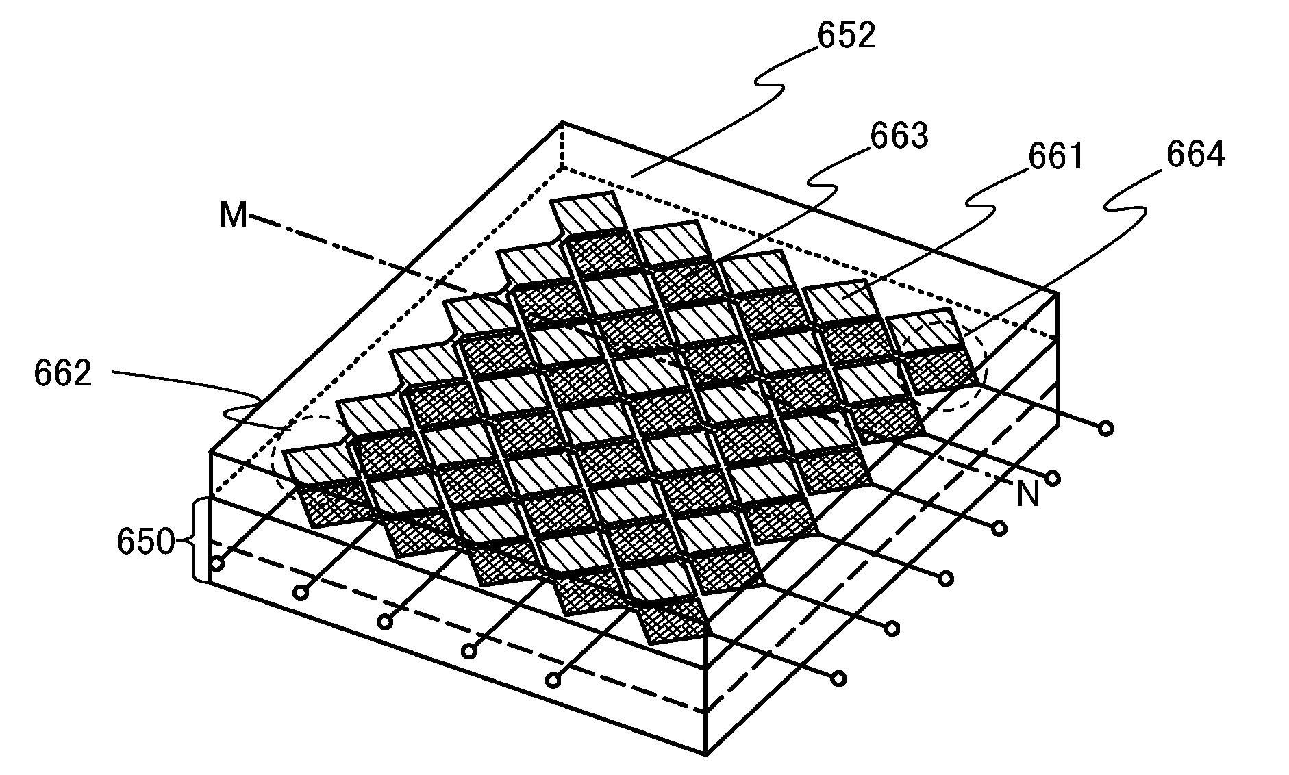
[0053]FIGS. 5A and 5B illustrate a shutter panel 500. FIG. 5A is a plan view of the shutter panel 500. FIG. 5B is a cross-sectional view along Y1-Y2 in FIG. ...

embodiment 3

[0072]In this embodiment, examples of the structure of a display panel applicable to the display panel in Embodiment 1 will be described with reference to FIGS. 7A and 7B and FIGS. 8A and 8B.

[0073]As a display element provided in the display panel, a light-emitting element (also referred to as a light-emitting display element) or a liquid crystal element (also referred to as a liquid crystal display element) can be used. A light-emitting element includes, in its category, an element whose luminance is controlled by current or voltage, and specifically includes an inorganic electroluminescent (EL) element, an organic EL element, and the like.

[0074]FIGS. 7A and 7B illustrate an example of the structure of a display panel in which an organic EL element is used as a display element. FIG. 7A is a plan view of the display panel. FIG. 7B is a cross-sectional view along A-B and C-D in FIG. 7A. An element substrate 410 is fixed to a sealing substrate 404 with a sealant 405, and includes driv...


PUM


Abstract

A display device includes a display panel including a matrix of pixel regions, and a shutter panel including a matrix of optical shutter regions each of which state is selected from a light-transmitting state and a light-shielding state. In a first display state, the display panel performs display regarding one pixel region as a display element unit, and each of the plurality of optical shutter regions in the shutter panel is brought into a light-transmitting state or a light-shielding state. In a second display state, the display panel performs display regarding at least two pixel regions as the display element unit, and each of the plurality of optical shutter regions in the shutter panel is brought into a light-transmitting state or a light-shielding state. As a result, the range of distance with which 3D images can be displayed can differ between the first display state and the second display state.

Description

BACKGROUND OF THE INVENTION[0001]1. Field of the Invention[0002]The present invention relates to display devices and particularly relates to a display device capable of displaying three-dimensional (3D) images.[0003]2. Description of the Related Art[0004]Display devices are widely used, ranging from large display devices such as television devices to small display devices such as mobile phones. High value-added products will be needed and are being developed. In recent years, display devices that can display 3D images have been developed in order to display more realistic images.[0005]As methods for displaying 3D images, there are a method using glasses for separating an image seen with a left eye and an image seen with a right eye (also referred to as stereoscopy), and autostreoscopy by which 3D images can be seen by the naked eye by addition of a structure for separating an image seen with a left eye and an image seen with a right eye in a display portion. It is not necessary to p...

Claims


Application Information

Patent Timeline
Patent Type & Authority Applications(United States)
IPC IPC(8): G06T15/00G02B30/31
CPCH04N13/0409H04N13/0413G02B27/2214H04N13/0468H04N13/0422H04N13/31H04N13/315H04N13/324H04N13/366G02B30/31G02F1/13G02B30/00G02B30/27
Inventor YAMAZAKI, SHUNPEIKOYAMA, JUN
Owner SEMICON ENERGY LAB CO LTD
Why Eureka
Try Eureka