Dual-depth self-aligned isolation structure for a back gate electrode

a self-aligning isolation and back gate electrode technology, applied in the field of semiconductor structure, can solve the problems of shallow trenches to an excessive depth, and is not practical to implement in advanced semiconductor devices having small dimensions, and achieve the effect of providing self-alignment between the back gate electrode and the back gate electrod

Inactive Publication Date: 2012-10-11
IBM CORP
View PDF6 Cites 190 Cited by
  • Summary
  • Abstract
  • Description
  • Claims
  • Application Information

AI Technical Summary

Problems solved by technology

Conventional schemes that employ back gate electrodes do not provide self-alignment between a back gate electrode and active areas thereabove because the back gate electrode is patterned separatel

Method used


Image

  • Dual-depth self-aligned isolation structure for a back gate electrode
  • Dual-depth self-aligned isolation structure for a back gate electrode
  • Dual-depth self-aligned isolation structure for a back gate electrode

Examples


Embodiment Construction

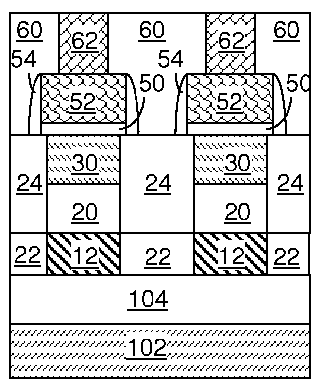
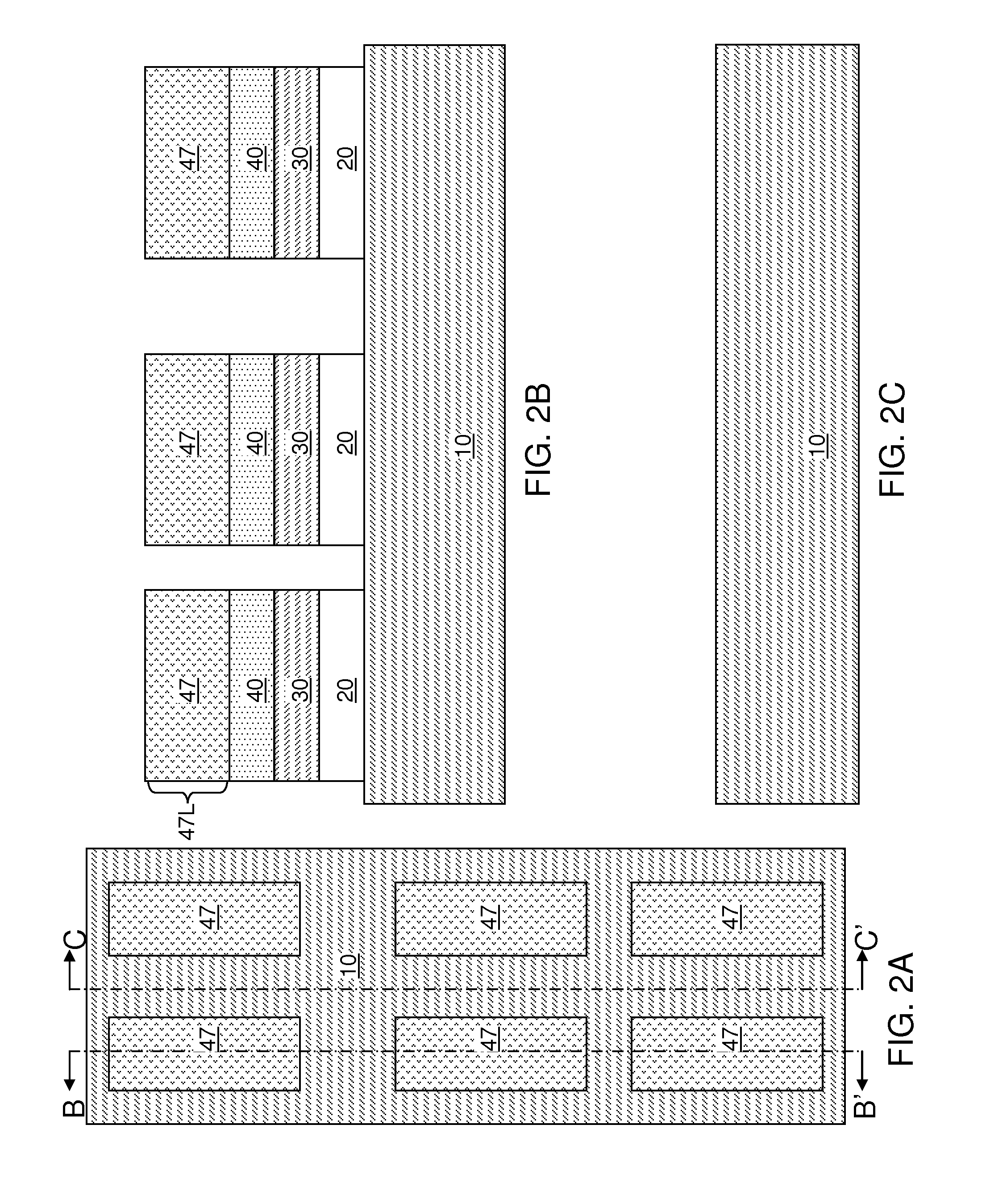
[0018]As stated above, the present disclosure relates to a semiconductor structure having dual isolation structures and a doped semiconductor back gate region self-aligned to at least one overlying active area, and methods of manufacturing the same, which are now described in detail with accompanying figures. It is noted that like reference numerals refer to like elements across different embodiments. The drawings are not necessarily drawn to scale.

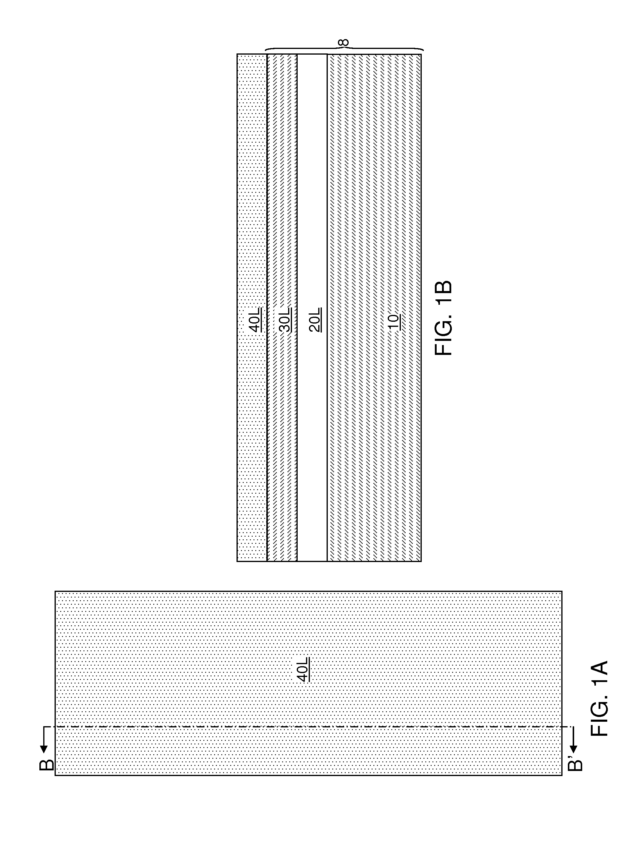
[0019]Referring to FIGS. 1A and 1B, a first exemplary semiconductor structure according to a first embodiment of the present disclosure includes a semiconductor-on-insulator (SOI) substrate 8. The SOI substrate 8 includes a stack of an underlying semiconductor layer 10, a buried insulator layer 20L, and a top semiconductor layer 30L. The underlying semiconductor layer 10 functions as a handle substrate, i.e., a substrate that provides mechanical support during handling of the SOI substrate 8. The underlying semiconductor layer 10 includes...


PUM


Abstract

Doped semiconductor back gate regions self-aligned to active regions are formed by first patterning a top semiconductor layer and a buried insulator layer to form stacks of a buried insulator portion and a semiconductor portion. Oxygen is implanted into an underlying semiconductor layer at an angle so that oxygen-implanted regions are formed in areas that are not shaded by the stack or masking structures thereupon. The oxygen implanted portions are converted into deep trench isolation structures that are self-aligned to sidewalls of the active regions, which are the semiconductor portions in the stacks. Dopant ions are implanted into the portions of the underlying semiconductor layer between the deep trench isolation structures to form doped semiconductor back gate regions. A shallow trench isolation structure is formed on the deep trench isolation structures and between the stacks.

Description

BACKGROUND[0001]The present disclosure generally relates to a semiconductor structure, and particularly to a semiconductor structure having dual isolation structures and a doped semiconductor back gate region self-aligned to at least one overlying active area, and methods of manufacturing the same.[0002]Back gate biasing is a useful method for adaptive power management. Planar fully depleted semiconductor-on-insulator (SOI) devices with a thin buried oxide layer (BOX) can be employed to introduce a back gate bias voltage that can independently control device performance without requiring changes to settings at other device nodes. For back gate biasing to be area-efficient, i.e., to provide a back gate biasing scheme that does not require an excessive device area, a group of transistors having the same polarity and target threshold voltage should share a single back gate electrode. However, each back gate electrode should be electrically isolated from adjacent transistors or any back...

Claims


Application Information

Patent Timeline
IPC IPC(8): H01L29/78H01L21/336
CPCH01L21/26506H01L21/2652H01L21/26586H01L21/84H01L21/76229H01L29/78648H01L21/743H01L29/66742H01L27/1203H01L21/2658
Inventor CHENG, KANGGUOHARAN, BALASUBRAMANIAN S.KHAKIFIROOZ, ALISHAHIDI, GHAVAM G.
Owner IBM CORP
Why Eureka
Try Eureka