Organic light emitting diode pixel circuit
a light-emitting diode and organic technology, applied in the field of organic light-emitting diode (oled) pixel circuits, can solve the problems of display brightness deterioration, increase in the threshold turn-on voltage of the oled element,
- Summary
- Abstract
- Description
- Claims
- Application Information
AI Technical Summary
Benefits of technology
Problems solved by technology
Method used
Image
Examples
first embodiment
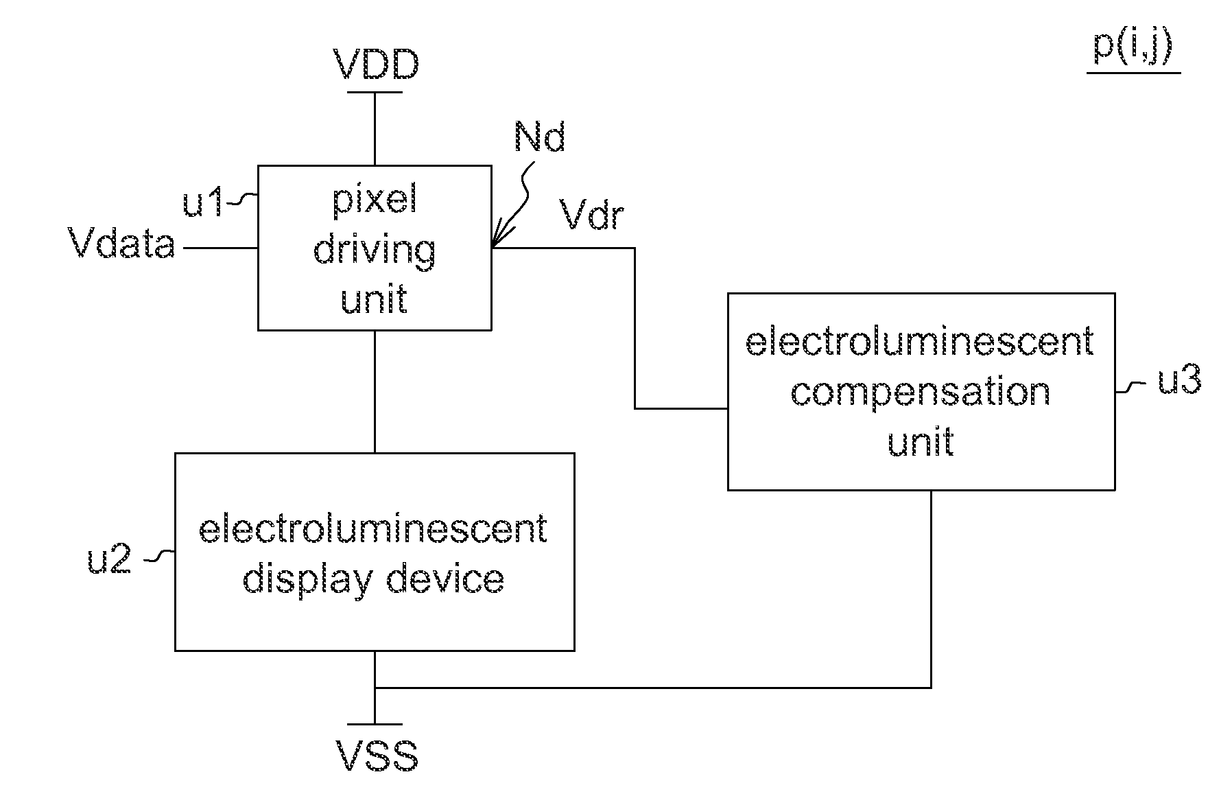
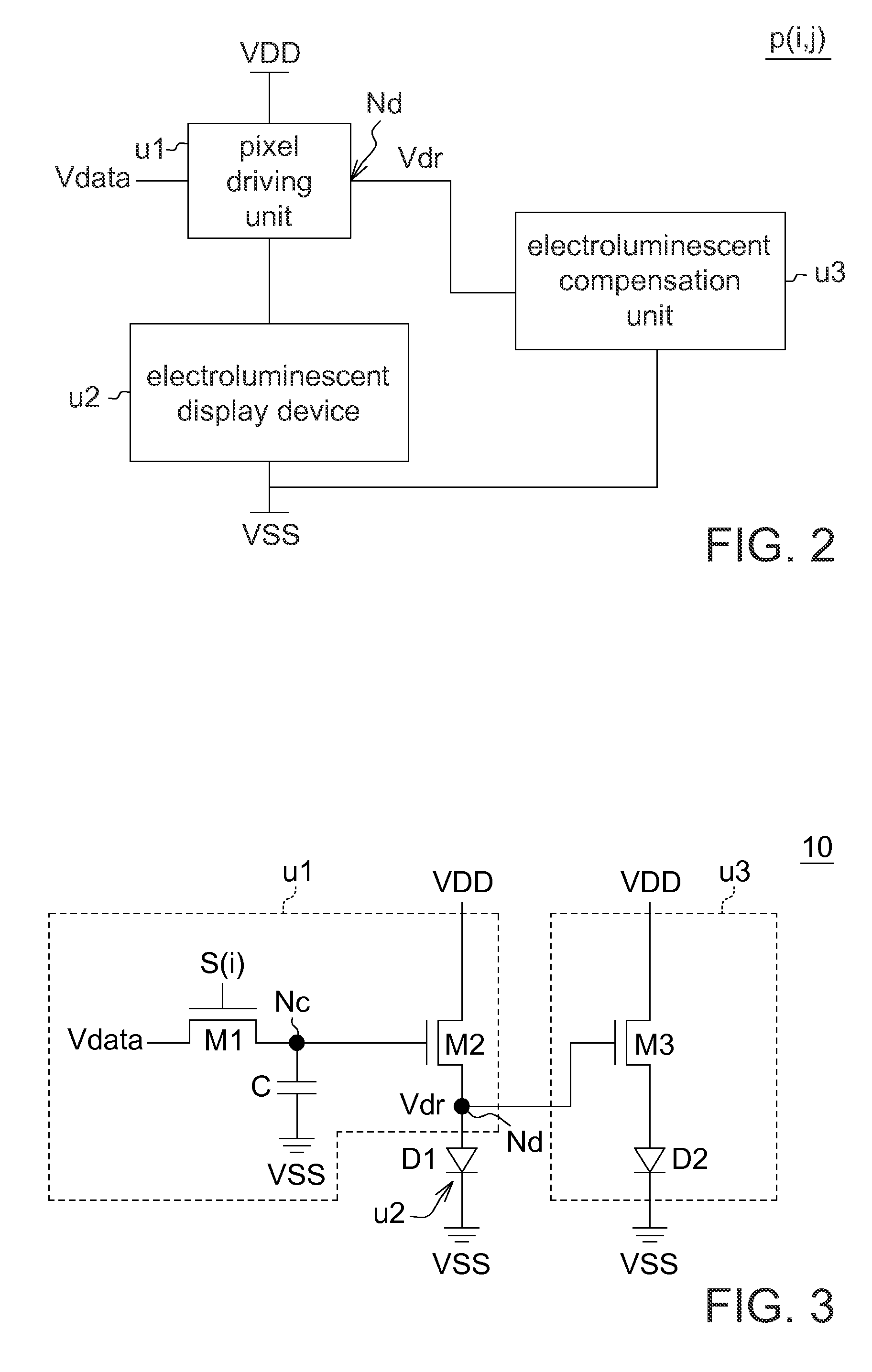
[0024]Referring to FIG. 3, a detailed circuit diagram of an OLED pixel circuit according to a first embodiment of the invention is shown. In the OLED pixel circuit 10 of the present embodiment of the invention, the pixel driving unit u1, having a 2T1C circuit structure, includes a node Nc, transistors M1˜M2 and a capacitor C. The electroluminescent display device u2 includes an OLED element D1. The electroluminescent compensation unit u3 includes a transistor M3 and an OLED element D2, wherein the OLED element D2 realizes the electroluminescent compensation element, and the transistor M3 realizes the auxiliary driving unit.
[0025]Furthermore, the transistors M1˜M2 are such as N-type metal oxide semiconductor (MOS) transistors. Of the transistor M1, the gate receives a current-stage scanning signal S(i), the source is coupled to node Nc, and the drain is coupled to the data line for receiving a data voltage Vdata. Of the transistor M2, the gate is coupled to node Nc, the drain receive...
second embodiment
[0036]Referring to FIG. 4, a circuit diagram of an OLED pixel circuit according to a second embodiment of the invention is shown. The OLED pixel circuit 20 of the present embodiment of the invention is different from the OLED pixel circuit 10 of the first embodiment in that the manufacturing of the transistors adopts the LTPS process, such that all the transistors are P-type MOS transistors.
[0037]Let the electroluminescent compensation unit u3 be taken for example. Of the transistor M13, the gate receives a low-potential reference voltage VSS, and the drain is coupled to the positive end of the OLED element D2. Of the OLED element D2, the negative end is coupled to a terminal end which receives a low-level reference voltage VSS. Of the transistor M13, the source is coupled to the driving node Nd for receiving a driving voltage Vdr. Before the OLED pixel circuit 20 is under the stress effect, the positive end voltage of the OLED element D1 is used a power supply for the electrolumine...
third embodiment
[0039]Referring to FIG. 5, a circuit diagram of an OLED pixel circuit according to a third embodiment of the invention is shown. The OLED pixel circuit 30 of the present embodiment of the invention is different from the OLED pixel circuit 10 of the first embodiment in that the pixel driving unit u1 has a different circuit structure. Furthermore, the pixel driving unit u1 of the present embodiment of the invention includes nodes Nc1 and Nc2, transistors M21˜M25 and a capacitor C, wherein transistors M21˜M25 are such as NMOS transistors.
[0040]Of the transistor M21, the gate receives a current-stage scanning signal S(i), the drain is coupled to the data line for receiving a data voltage Vdata, and the source is coupled to the node Nc1. Of the transistor M22, the gate receives a current-stage scanning signal S(i), the drain is coupled to node Nc1, and the source is coupled to node Nc2. Of the transistor M23, the gate is coupled to node Nc2, the drain is coupled to node Nc1, and the sour...
PUM
 Abstract
Description
Claims
Application Information


