Method of joining a chip on a substrate

a technology of chip and substrate, applied in the direction of soldering apparatus, manufacturing tools, auxiliaries welding devices, etc., can solve the problems of substrate bending and warpage, failure of beol structure, and increasing the number of failures, so as to reduce or prevent bending and warping of substrates and chips, the effect of reducing or preventing bending and warping

Inactive Publication Date: 2012-11-22
ALSEPHINA INNOVATIONS INC
View PDF1 Cites 7 Cited by
  • Summary
  • Abstract
  • Description
  • Claims
  • Application Information

AI Technical Summary

Benefits of technology

[0016]The present disclosure provides a method and apparatus for assembling chips and substrates that reduces or prevents distortion such as bending and warping of the chip assembly. The present disclosure is useful in reducing or preventing bending and warping that can occur during the assembly of a chip or other electronic component onto a substrate, especially a flip chip assembly with organic substrates and chips that include low-k or ultralow-k materials. The present disclosure is especially useful in reducing or preventing bending and warping that can occur during a flip chip assembly process that heats and cools a chip assembly to bond a chip to a substrate. This is particularly useful in reducing or preventing distortion such as bending and warping that occur during a solder reflow process.
[0017]The disclosed methods and apparatuses reduce or eliminate distortions such as bending and warping that occur during chip assembly by providing a method and apparatus for restraining a substrate against the bending and warping stresses and strains that occur during chip assembly. In particular, the present disclosure provides a method and apparatus for applying a variable mechanical force and pressure to a substrate during the chip assembly process. This pressure is applied to at least a portion of the top surface and at least a portion of the bottom surface of the substrate to prevent or reducing bending and warping.
[0021]Distortions such as bending and warping of the chip assembly, including the substrate and the chip, can be reduced or prevented by the present disclosure, particularly the bending and warping that occur during assembly of a chip onto an organic substrate by a solder reflow process. This reduces or prevents opens and shorts in the chip assembly.
[0023]The disclosed methods and apparatuses reduce or prevent bending and warping in substrates such as ceramic and silicon substrates. They also reduce or prevent bending and warping within the BEOL structure of a chip, and cracking or delamination of the BEOL structure of a chip, and even cohesive failure between the layers of a chip, particularly during a solder reflow process. This is very useful for larger chips and coreless substrate technologies, which can bend and warp more than thincore substrates.
[0024]Another advantage of the disclosed methods and apparatuses is that they can be used during assembly of chips and substrates of any dimensions, including multiple chips and multiple substrates, to reduce or prevent bending and warping of the substrates and chips, including internal bending and warping of the BEOL structure of the chip.

Problems solved by technology

However, when organic substrates are used for the flip chip assembly, substrate bending and warpage can occur.
The thermally-induced stress / strain in the flip-chip structure often results in a failure of the BEOL structure.
This failure is becoming more common because low k dielectric layers are more fragile than solder joints.
They can impair the electrical and mechanical connections between the flip chip 100 and the substrate 106, and degrade the performance of the flip chip assembly.
This arrangement does not effectively control the thermal-mechanical stresses that occur during chip assembly, particularly during a solder reflow process, and can increase the stress or strain that develops in the chip.

Method used


Image

  • Method of joining a chip on a substrate
  • Method of joining a chip on a substrate
  • Method of joining a chip on a substrate

Examples


Embodiment Construction

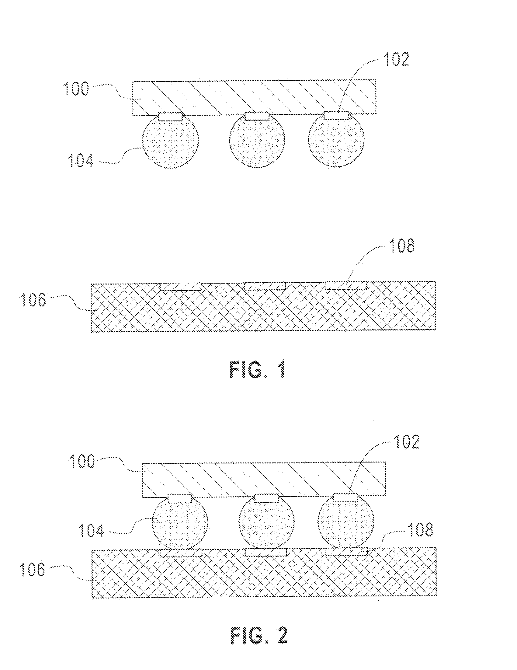
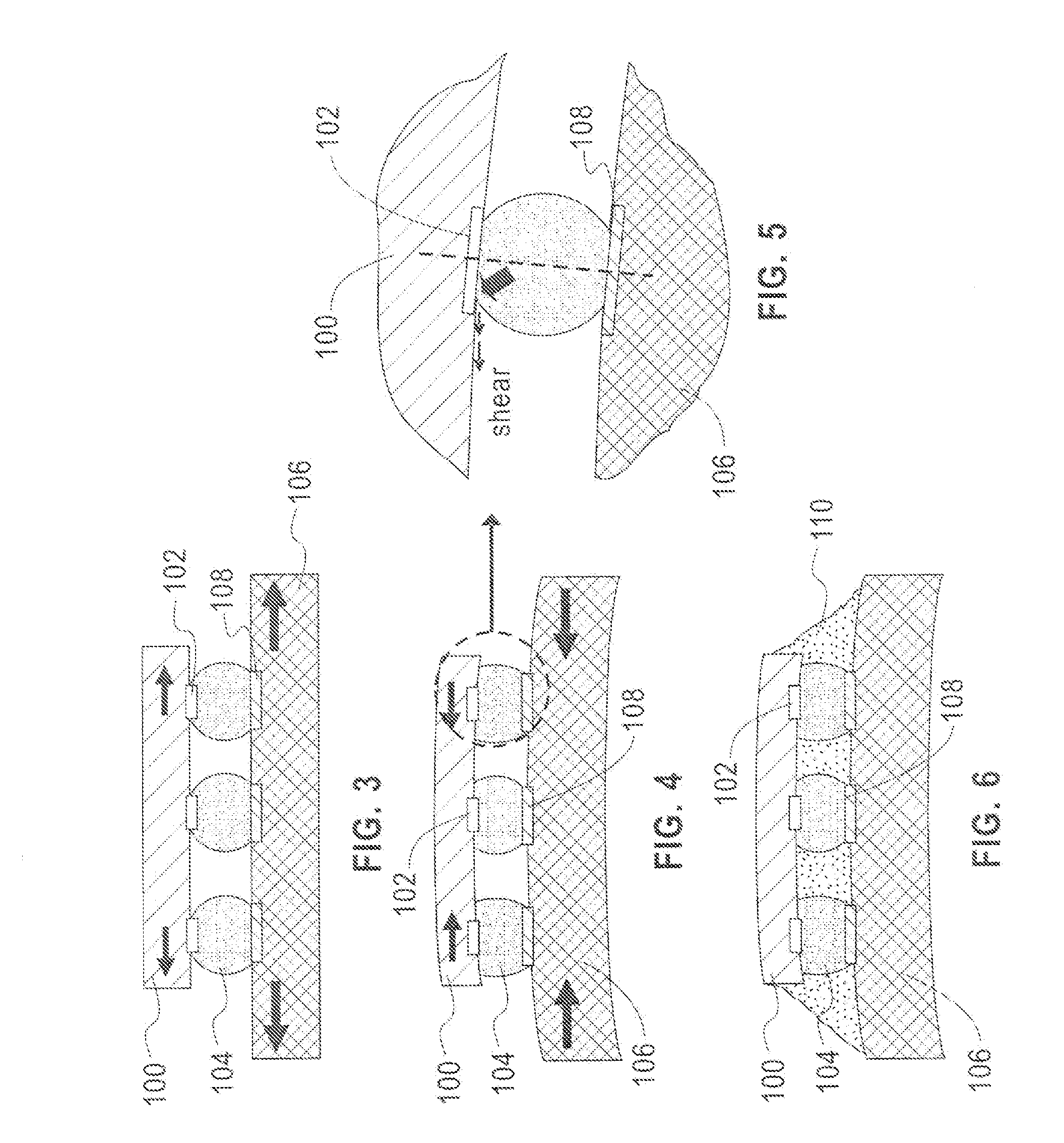
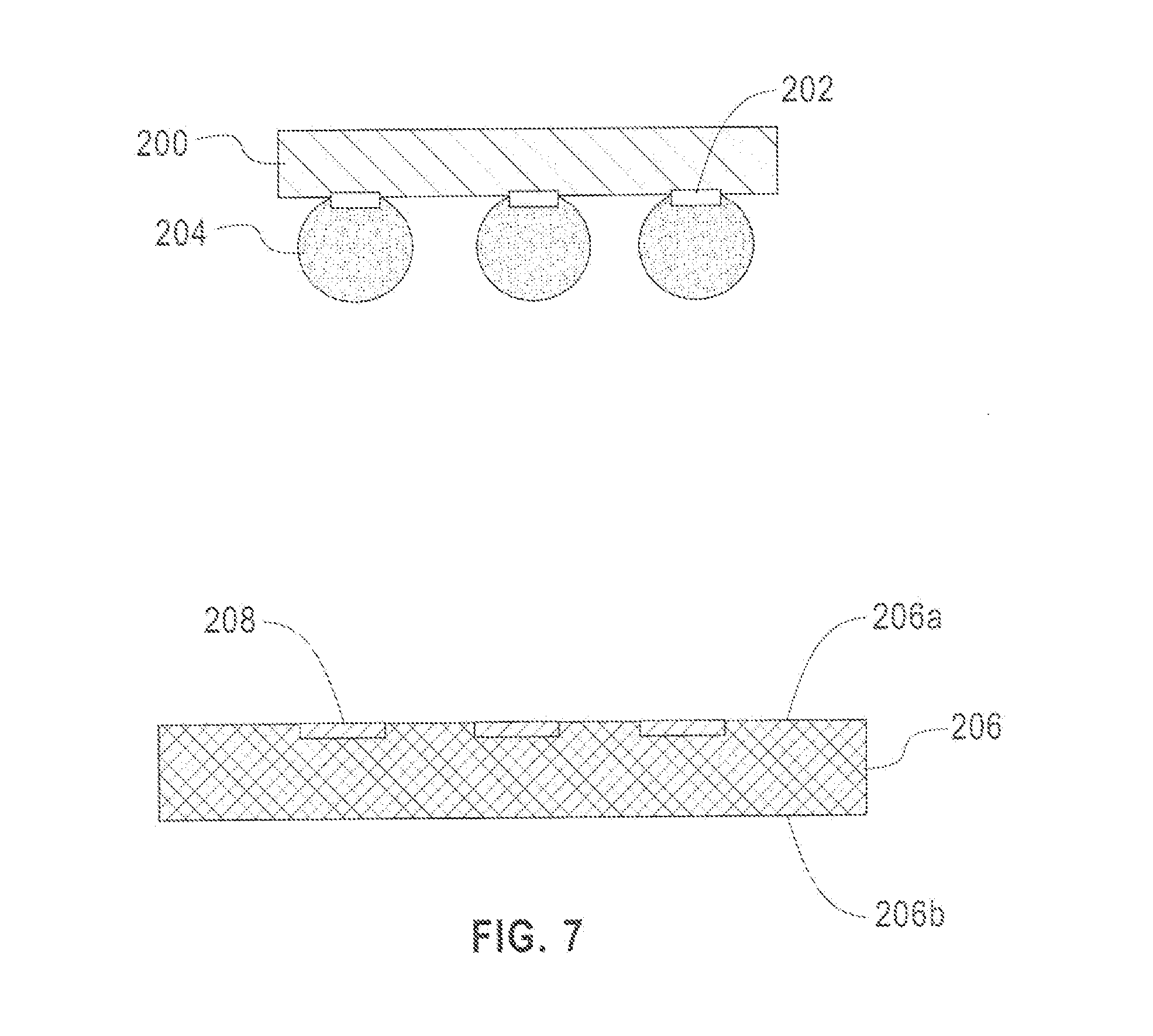
[0061]According to a preferred embodiment, a chip 200 and a substrate 206 are assembled by a flip chip assembly process. As shown in FIG. 7, the chip 200, which may be a silicon chip, includes a plurality of bump limiting metallurgy contacts (BLM) 202 formed or placed on a surface of the chip 200. The BLM 202 typically correspond to I / Os of the chip 200. A bump 204, such as a solder bump, is disposed on each BLM 202. A substrate, such as an organic substrate 206, includes a top surface 206a and a bottom surface 206b. The substrate 206 includes four lateral edges 206c, 206d, 206e, 206f, as shown in FIGS. 8 and 9. The substrate 206 includes a plurality of conductive pads 208 disposed along the top surface 206a of the substrate 206. The bumps 204 can be applied by any means, for example by evaporation, electroplating, direct placement (ball drop), IMS (C4NP), and the like.

[0062]The substrate 206 is positioned on a carrier 210 so that the bottom surface 206b of the substrate 206 contact...


PUM

PropertyMeasurementUnit
melting pointsaaaaaaaaaa
melting pointaaaaaaaaaa
pressureaaaaaaaaaa

Abstract

A method and apparatus for making chip assemblies is disclosed that prevent or reduce the cracking and delamination of ultra low-k dielectrics in the back-end-of-line in Si chips that can occur during the chip assembly process. The method and apparatus apply pressure to the top and bottom surfaces of a substrate during the chip bonding process so that the bending and warping of the assembled modules are reduced. The reduced bending and warping prevent or reduce the cracking and delamination of ultra low-k dielectrics.

Description

CROSS REFERENCE TO RELATED APPLICATION[0001]This application is a divisional of co-pending application Ser. No. 12 / 551,960, filed on Sep. 1, 2009, and for which priority is claimed under 35 U.S.C. §120; the entire contents of which is are hereby incorporated by reference.[0002]The present invention relates to a method and apparatus of making a chip assembly by bonding a chip or other electronic component to a substrate. In particular, the present invention discloses a method and apparatus for assembling a silicon (Si) chip onto an organic substrate while applying mechanical force to the organic substrate to eliminate cracking or delamination in back end of line (BEOL) structure of the Si chip by reducing or preventing warping or bending of the organic substrate.BACKGROUND[0003]Flip chip is the name of a process in which a semiconductor Si chip is flipped over so that the connection pads face towards the substrate. Flip chip technology was first introduced by IBM in the solid logic t...

Claims


Application Information

Patent Timeline
Patent Type & Authority Applications(United States)
IPC IPC(8): B23K37/04
CPCB23K1/0016H01L21/563H01L2224/131H01L2924/10253H01L2924/014H01L2924/01076H01L2924/0105H01L24/75H01L24/81H01L2224/13099H01L2224/73204H01L2224/75704H01L2224/75985H01L2224/81005H01L2224/81191H01L2224/81815H01L2224/8191H01L2924/01029H01L2924/01082H01L2924/01322H01L2924/3511H01L2924/01006H01L2924/01019H01L2924/01033H01L2924/01047H01L2924/01026H01L2924/00H01L2924/15787
Inventor BLAIS, PASCAL P.FORTIER, PAUL F.LEE, KANG-WOOKNAH, JAE-WOONGPARK, SOOJAETOUTANT, ROBERT L.WARREN, ALAIN A.
Owner ALSEPHINA INNOVATIONS INC
Why Eureka
Try Eureka