Fin-fet device and method and integrated circuits using such

a technology of field effect transistors and fins, applied in solid-state devices, basic electric elements, electric devices, etc., can solve the problems of specific performance criteria, fin-fets and ics embodied by fin-fets, and special challenges

Inactive Publication Date: 2012-12-13
ALSEPHINA INNOVATIONS INC
View PDF2 Cites 67 Cited by
  • Summary
  • Abstract
  • Description
  • Claims
  • Application Information

AI Technical Summary

Benefits of technology

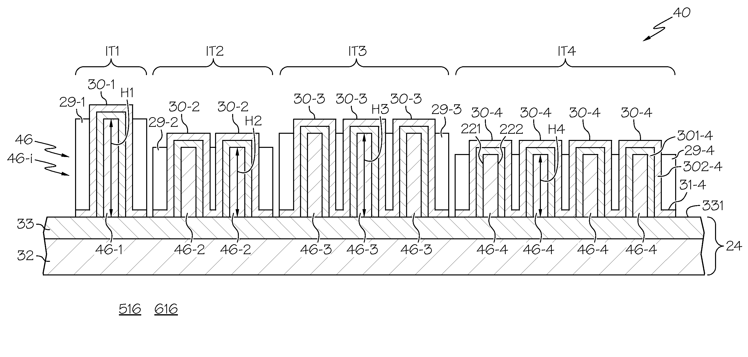
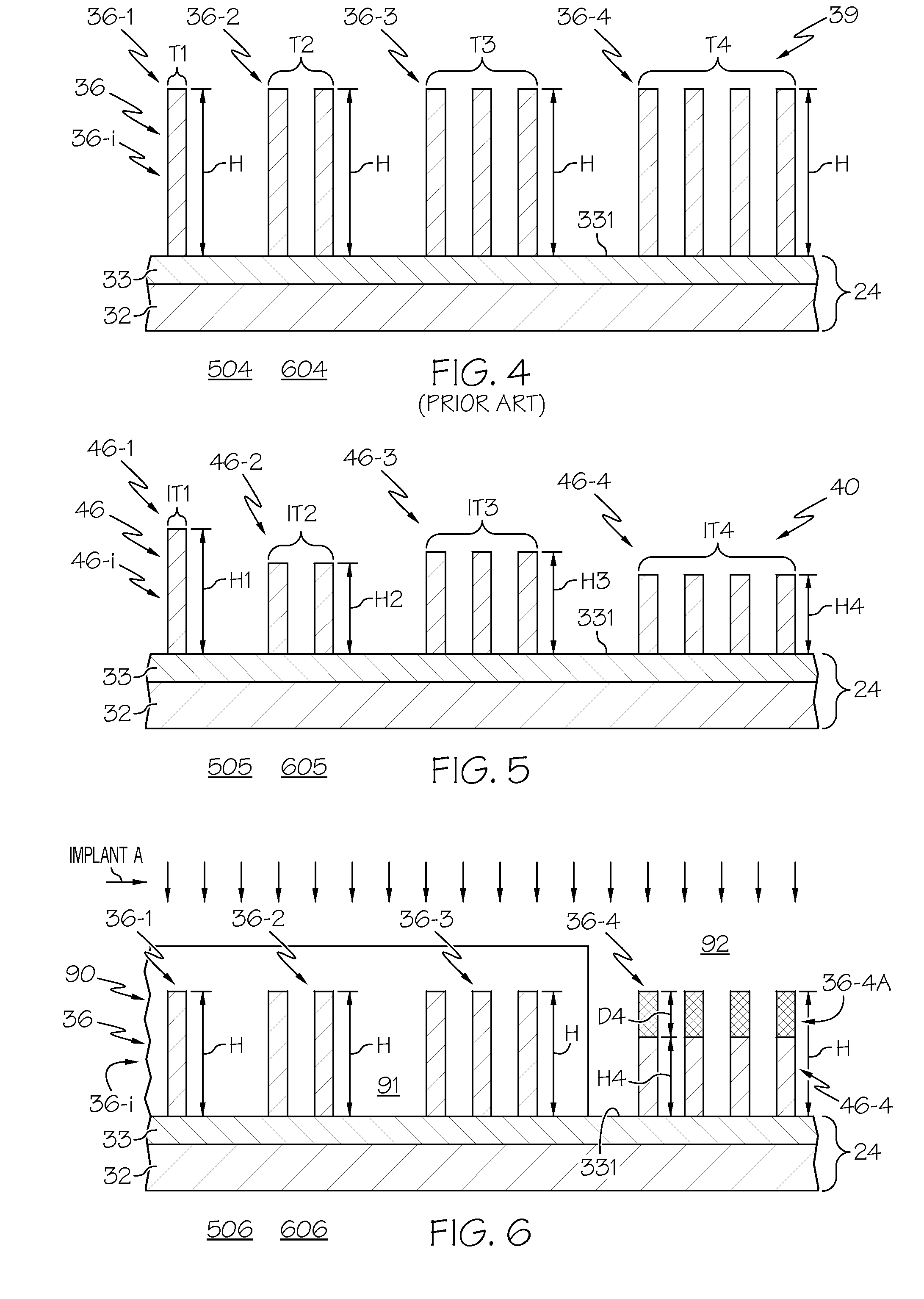
[0004]A method is provided for forming an integrated circuit (IC) having field effect transistors (FET's) whose conductive channels lie in fins standing substantially perpendicular to a supporting substrate. Such FETs are hereafter referred to as FIN-FETs. The method includes, providing a substrate having thereon semiconductor fins of first fin height H1 and other semicond...

Problems solved by technology

Because of the distinctly different geometry of a FIN-FET compared to a planar FET, designing and const...

Method used


Image

  • Fin-fet device and method and integrated circuits using such
  • Fin-fet device and method and integrated circuits using such
  • Fin-fet device and method and integrated circuits using such

Examples


Embodiment Construction

[0018]The following detailed description is merely exemplary in nature and is not intended to limit the invention or the application and uses of the invention. Furthermore, there is no intention to be hound by any expressed or implied theory presented in the preceding technical field, background, or the following detailed description. For simplicity and clarity of illustration, the drawing figures illustrate the general manner of construction, and descriptions and details of well-known features and techniques may be omitted to avoid unnecessarily obscuring the invention. Additionally, elements in the drawings figures are not necessarily drawn to scale. For example, the dimensions of some of the elements or regions in the figures may be exaggerated relative to other elements or regions to help improve understanding of embodiments of the invention.

[0019]The terms “comprise,”“include,”“have” and any variations thereof, are intended to cover non-exclusive inclusions, such that a process...


PUM


Abstract

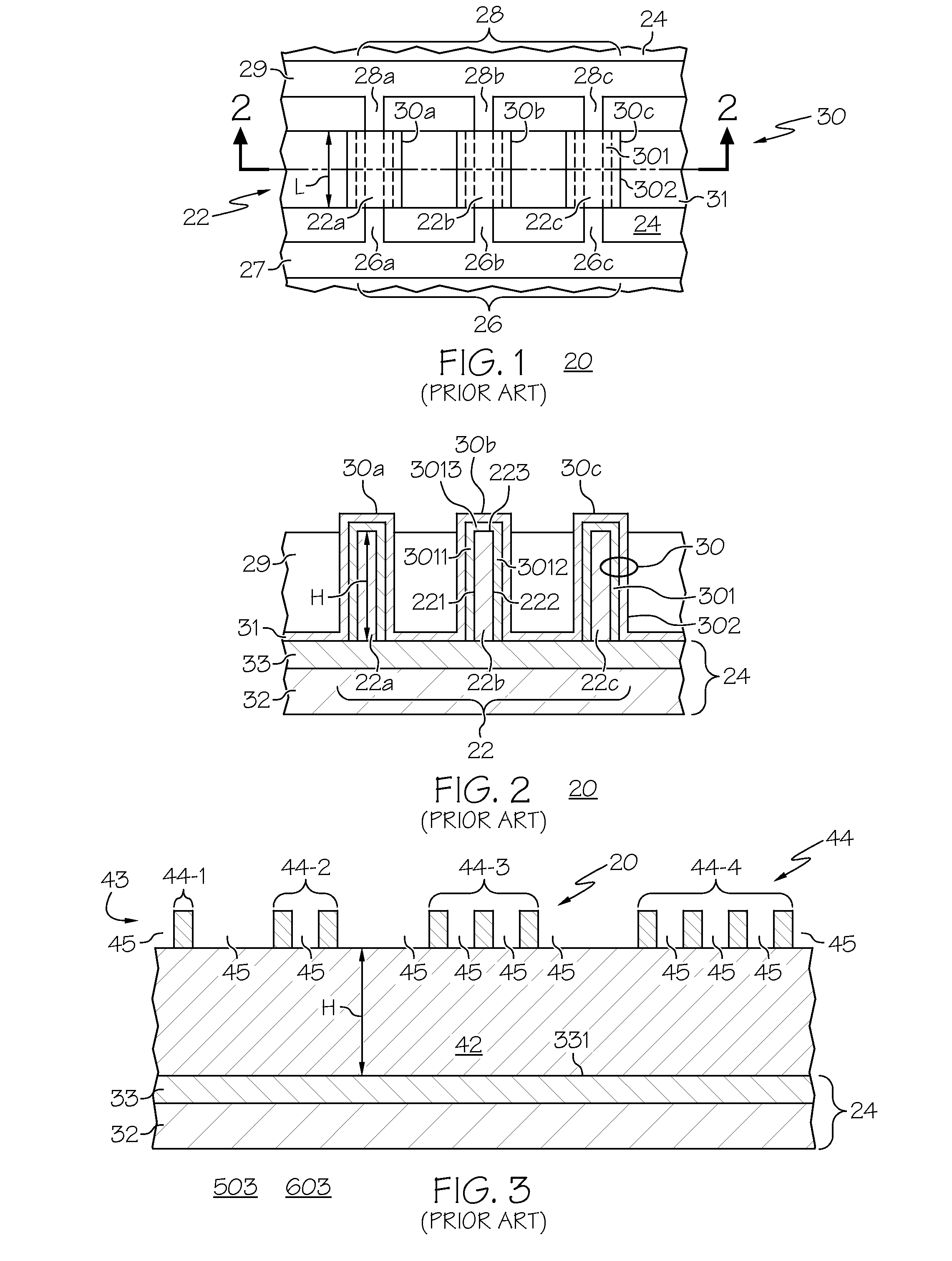
FIN-FET ICs with adjustable FIN-FET channel widths are formed from a semiconductor layer (42). Fins (36) may be etched from the layer (42) and then some (46) locally shortened or the layer (42) may be locally thinned and then fins (46) of different fin heights etched therefrom. Either way provides fins (46) and FIN-FETs (40) with different channel widths W on the same substrate (24). Fin heights (H) are preferably shortened by implanting selected ions (A, B, C, etc.) through a mask (90, 90′, 94, 94′, 97, 97′) to locally enhance the etch rate of the layer (42) or some of the fins (36). The implant(s) (A, B, C, etc.) is desirably annealed and then differentially etched. This thins part(s) (42-i) of the layer (42) from which the fins (46) are then etched or shortens some of the fins (46) already etched from the layer (42). For silicon, germanium is a suitable implant ion. Having fins (42) with adjustable fin heights Hi on the same substrate (24) enables such FIN-FET ICs (40) to avoid channel-width quantization effects observed with prior art uniform fin height FIN-FETs (20).

Description

FIELD OF THE INVENTION[0001]This invention relates generally to structures and methods for forming fins for fin-type field effect transistors (FIN-FETs), the FIN-FETs using such fins and integrated circuits (ICs) incorporating such FIN-FETs.BACKGROUND OF THE INVENTION[0002]It is known that high performance field effect transistors (FETs) can be formed in fin-like semiconductor structures, commonly referred to as “FIN-FETs”. Integrated circuits (ICs) are fabricated using such FIN-FETS. Unlike conventional planar FETs, with FIN-FETs the semiconductor region containing the source-drain channel has a fin-like shape standing approximately perpendicular to the plane of the substrate die or wafer on which the device is formed. Gate electrodes can be provided on both exposed sides of the fin-like channel region and sometimes along the narrow top edge and even along the narrow bottom edge, although such edge gates are not required. The term “tri-gate” is used to refer to fin-type FETs that h...

Claims


Application Information

Patent Timeline
IPC IPC(8): H01L27/12H01L21/66H01L21/84
CPCH01L21/823431H01L22/20H01L22/12H01L21/845
Inventor WAHL, JEREMYMAITRA, KINGSUK
Owner ALSEPHINA INNOVATIONS INC
Why Eureka
Try Eureka