Lighting Device and Liquid Crystal Display Using the Same

Active Publication Date: 2013-01-31
LG INNOTEK CO LTD
View PDF14 Cites 29 Cited by
  • Summary
  • Abstract
  • Description
  • Claims
  • Application Information

AI Technical Summary

Benefits of technology

[0029]According to exemplary embodiments of the present invention, it is advantageous that the improvement of luminance as well as the improvement of light reflectance can be maximized and luminance can be enhanced without an increase in a thickness of the lighting device or the number of light sources by providing the reflective unit having the air area on the surface of the printed circuit board, and thanks to a pattern design of the separation member (the spacer) which forms the air area, light control and reflection efficiency can be also maximized.
[0030]In particular, it is advantageous that a reflection rate of a surface of the metal layer which is the first reflective film or the element of white PET (polyethylen terephthalate) is improved to thereby maximize light efficiency by forming the first air area, which is an air layer area within the reflective unit, in a structure in which unit air cells may communicate with each other.
[0031]Furthermore, the present invention is provided with the effect that the optical pattern layer having an optical pattern is formed to have the air area by patterning the adhesive material (i.e. the adhesive pattern layer), so hot spots and dark spaces generated in a light shielding pattern part can be removed, reliability between components bonded to the adhesive material can be secured, a lightin

Problems solved by technology

However, due to a thickness of the light guide plate itself, there is a limitation to make a whole thickness of a

Method used


Image

  • Lighting Device and Liquid Crystal Display Using the Same
  • Lighting Device and Liquid Crystal Display Using the Same
  • Lighting Device and Liquid Crystal Display Using the Same

Examples


first exemplary embodiment

1. First Exemplary Embodiment

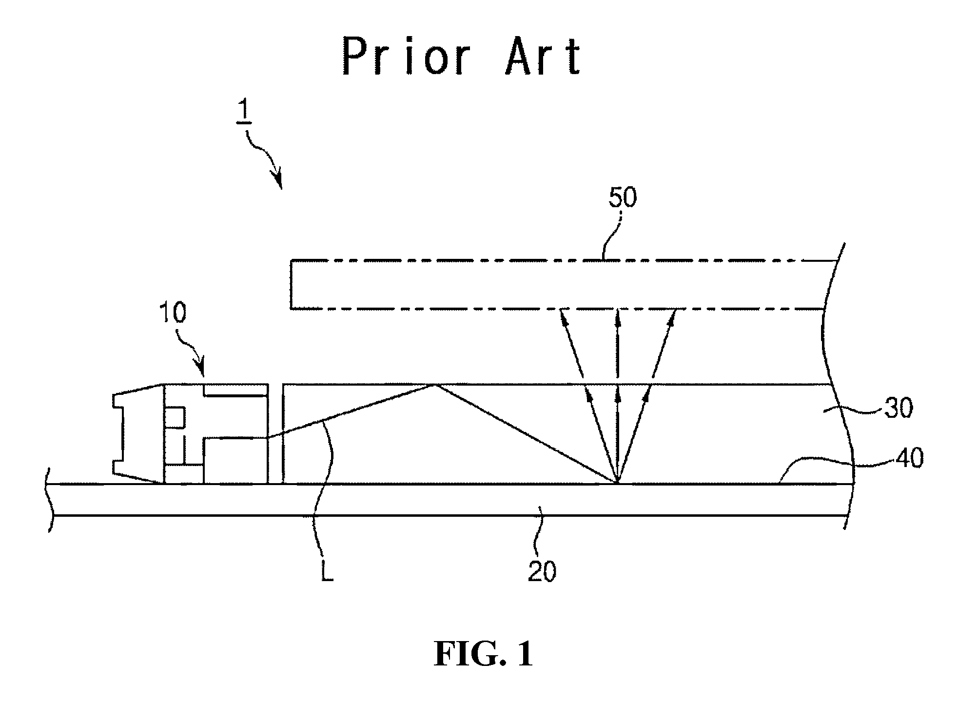
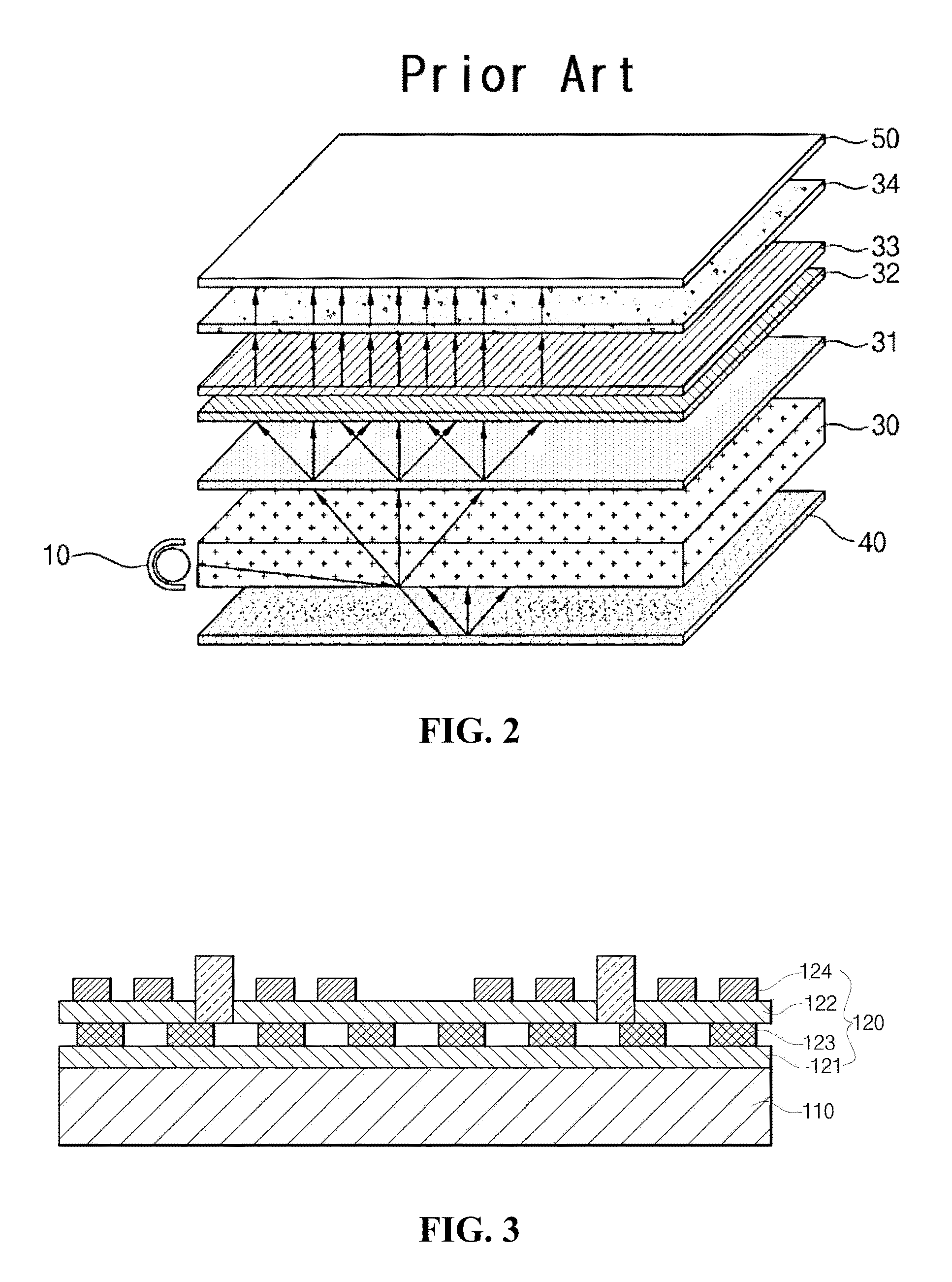
[0048]FIG. 3 is a cross-section conceptual view illustrating the subject matter of a lighting device according to an exemplary embodiment of the present invention. FIG. 4 is an enlarged view of the subject matters for explaining the detailed configuration of the reflective unit in the structure of FIG. 3.

[0049]Referring to FIG. 3, the lighting device according to the exemplary embodiment of the present invention may include: a plurality of LED light sources 130 formed on a printed circuit board 110; and a reflective unit 120 stacked on the printed circuit board 110 in a structure in which the LED light sources 130 penetrate, at an upper surface of the printed circuit board 110. In particular, in this case, an air area A1 is provided in an inner part of the reflective unit 120. The air area A1 may maximize luminance by improving the reflection efficiency of light emitted from the LED light sources 130. Particularly, the reflective unit 120 may include: a ...

second exemplary embodiment

2. Second Exemplary Embodiment

[0060]FIG. 8 illustrates the lighting device according another exemplary embodiment of the present invention.

[0061]That is, in addition to the structure of the aforesaid first exemplary embodiment, the second exemplary embodiment according to the present invention implements a structure in which a resin layer 140 is stacked on the printed circuit board. The configuration of the resin layer corresponds to the configuration which substitutes for a light guide plate of the lighting device, and functions to guide the light emitted from the light source forward.

[0062]Referring to FIG. 8, the lighting device according to the present exemplary embodiment of the invention may further include the plurality of LED light sources 130 formed on the printed circuit board 110, and the resin layer 140 for diffusing and guiding emitted light forward. That is, the resin layer 140 is stacked in a structure surrounding around the LED light sources and functions to disperse...

third exemplary embodiment

3. Third Exemplary Embodiment

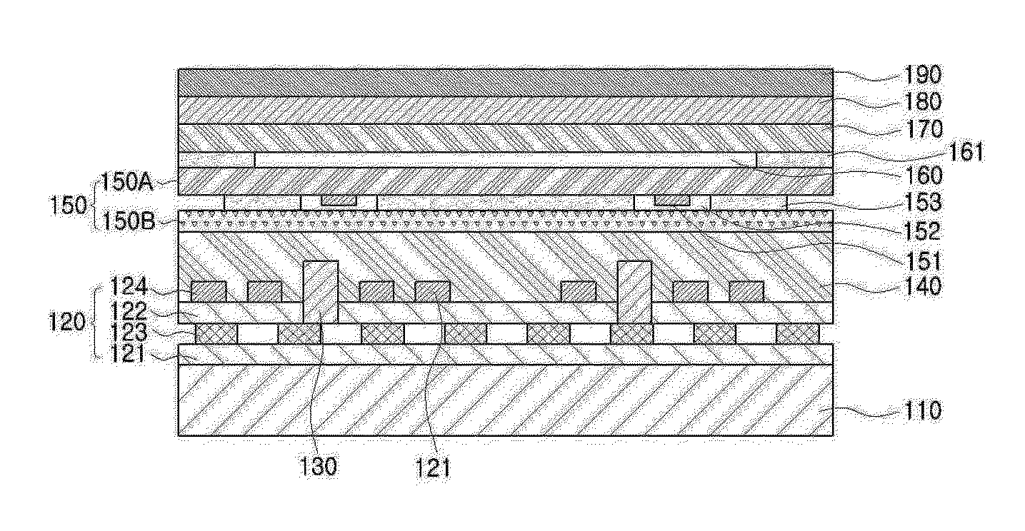
[0066]As an improved structure from the aforesaid structure of the second exemplary embodiment, a structure of the lighting device of the third exemplary embodiment in which the optical pattern layer for promoting the diffusion of light is implemented on the resin layer is explained.

[0067]That is, referring to FIG. 9, in the aforesaid structure of FIG. 8, the lighting device according to the present exemplary embodiment of the invention may be implemented in a structure in which an optical pattern layer 150 disposed on an upper part of the resin layer 140 and including an optical pattern 151 is provided.

[0068]In particular, the optical pattern layer 150 may be include a second pattern layer 153 which forms a second air area 152 surrounding around the optical pattern. That is, the second adhesive pattern layer 153 forms a spaced space (i.e. the second air area) having a pattern in a fixed shape in the optical pattern 151 and is implemented by applying and...


PUM

PropertyMeasurementUnit
Weightaaaaaaaaaa
Shapeaaaaaaaaaa
Areaaaaaaaaaaa

Abstract

Provided is a lighting device comprising: a plurality of LED light sources formed on a printed circuit board; and a reflective unit stacked on the printed circuit board in a structure in which the LED light sources penetrate, wherein the reflective unit comprises a first reflective film and a second reflective film disposed to oppose to each other, and a first adhesive pattern layer which bonds the first and second reflective films, and in which a plurality of unit air cells having a first air area formed in an inner part thereof are closely disposed to communicate with each other.
According to the present invention, it is advantageous that the improvement of luminance as well as the improvement of light reflectance can be maximized by providing the reflective unit having an air area to a surface of the printed circuit board.

Description

CROSS-REFERENCE TO RELATED APPLICATION[0001]This application claims the benefit under 35 U.S.C §119 of Korean Patent Application Nos. 10-2011-0076259, filed Jul. 29, 2011, and 10-2012-0017285, filed Feb. 21, 2012, which are hereby incorporated by reference in their entirety.BACKGROUND[0002]1. Field of the Invention[0003]The present invention relates to a lighting device using an LED as a lighting source, more specifically, to a backlight unit, a liquid crystal display device, and a lamp device for vehicles using the lighting device.[0004]2. Description of the Related Arts[0005]A device implementing lighting by guiding light emitting at a light source has been variously required for a lamp for lighting, a lamp for vehicles, a liquid crystal display device and the like. In the lighting device, a technology for making the structure of equipment thin, and a structure capable of improving light efficiency have been recognized as the most important technologies.[0006]As one example in whi...

Claims


Application Information

Patent Timeline
IPC IPC(8): F21V7/22G02F1/13357
CPCG02F2001/133628G02B6/0055B32B7/14G02F1/133512G02F1/133603B32B2307/416G02B5/124G02F2202/28B32B27/08B32B27/36G02F1/133605G02F1/133606G02F1/133628
Inventor PARK, MOO RYONGKIM, CHUL HONGLEE, BYOUNG EONPARK, KWANG HO
Owner LG INNOTEK CO LTD
Why Eureka
Try Eureka