ESD protection circuit
- Summary
- Abstract
- Description
- Claims
- Application Information
AI Technical Summary
Benefits of technology
Problems solved by technology
Method used
Image
Examples
Embodiment Construction
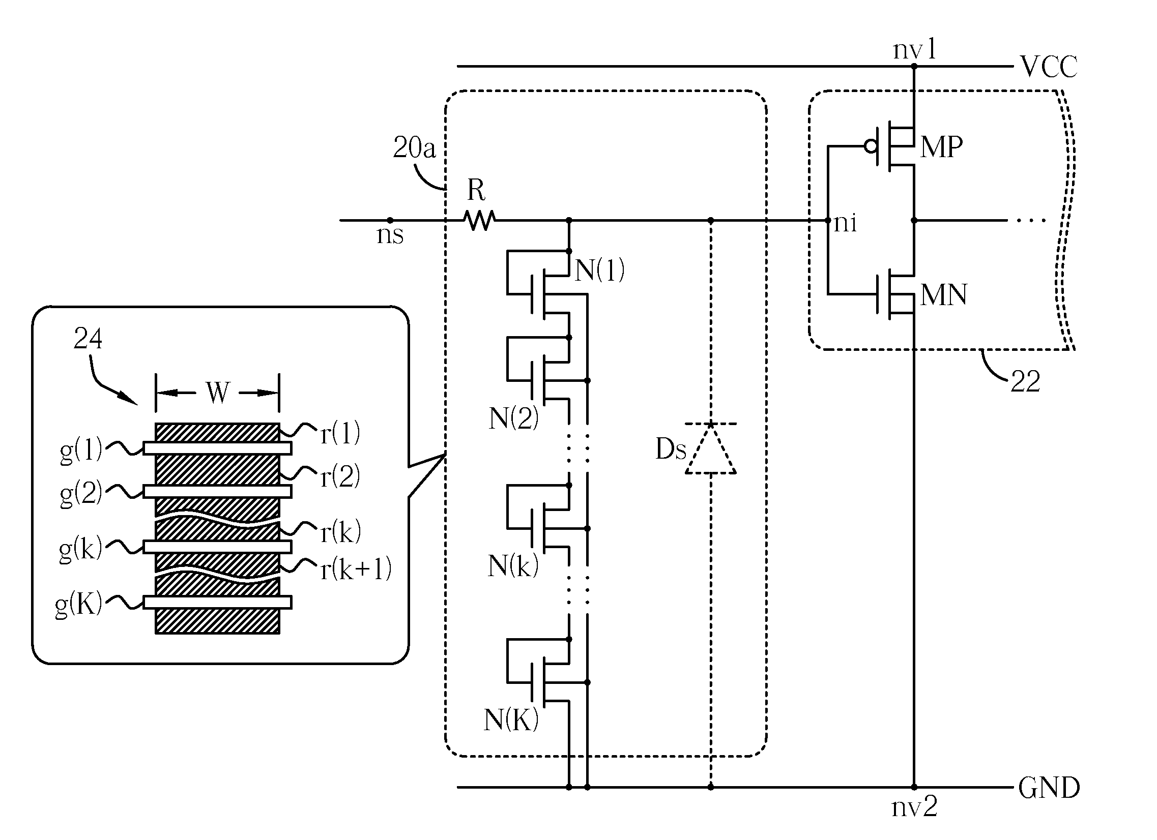
[0016]Please refer to FIG. 2 illustrating an ESD protection circuit 20a according to an embodiment of the invention; it can be implemented in a die to protect an internal circuit 22 of the die. For example, the internal circuit 22 includes two transistors MP (a p-channel MOS transistor) and MN (an n-channel MOS transistor), gates of them are commonly coupled to a node ni (an internal node) for receiving signal from signal routings of a node ns (a signal node). The signal can come from an input pad, or be a signal outputted to the node ns from another power domain. The internal circuit 22 are coupled to voltages VCC (power voltage) and GND (ground voltage) respectively by supply routings of nodes nv1 and nv2 (two voltage nodes); a source and a bulk of the transistor MN is coupled to the node nv2, a source and a bulk of the transistor MP is coupled to the node nv1. The transistors MN and MP can be transistors of thin gate-oxide, which occupy less area, respond faster and operate under...
PUM
 Abstract
Description
Claims
Application Information
 - R&D
- Intellectual Property
- Life Sciences
- Materials
- Tech Scout
- Unparalleled Data Quality
- Higher Quality Content
- 60% Fewer Hallucinations
Browse by: Latest US Patents, China's latest patents, Technical Efficacy Thesaurus, Application Domain, Technology Topic, Popular Technical Reports.
© 2025 PatSnap. All rights reserved.Legal|Privacy policy|Modern Slavery Act Transparency Statement|Sitemap|About US| Contact US: help@patsnap.com


