Transistor with self-aligned channel width

a technology of channel width and transistor, applied in the field of transistors, can solve the problems of shrinking the size of the transistor in the image pixels, increasing manufacturing costs, and affecting the isolation of conventional transistor technologies

Active Publication Date: 2013-04-25
OMNIVISION TECH INC
View PDF1 Cites 14 Cited by
  • Summary
  • Abstract
  • Description
  • Claims
  • Application Information

AI Technical Summary

Problems solved by technology

However, conventional transistor technologies encounter isolation challenges and increased manufacturing expenses as the size of the transistors in image pixels shrink.
LOCOS is suitable for image sensors, but it is difficult to reduce the size of the pixel with LOCOS technology.
However, both technologies create an isolation edge effect where the isolation region meets the active portion of a transistor.
The isolation edge effect can negatively influence the electrical characteristics of a transistor.
Tooling for fabrication becomes more and more expensive as transistors get smaller.
Reducing the size of a transistor requires tools with smaller tolerances and these precision tools increase manufacturing cost.
Another byproduct of manufacturing smaller transistors is higher defect rates due to misalignment of transistor structures in the fabrication process.

Method used


Image

  • Transistor with self-aligned channel width
  • Transistor with self-aligned channel width
  • Transistor with self-aligned channel width

Examples


Embodiment Construction

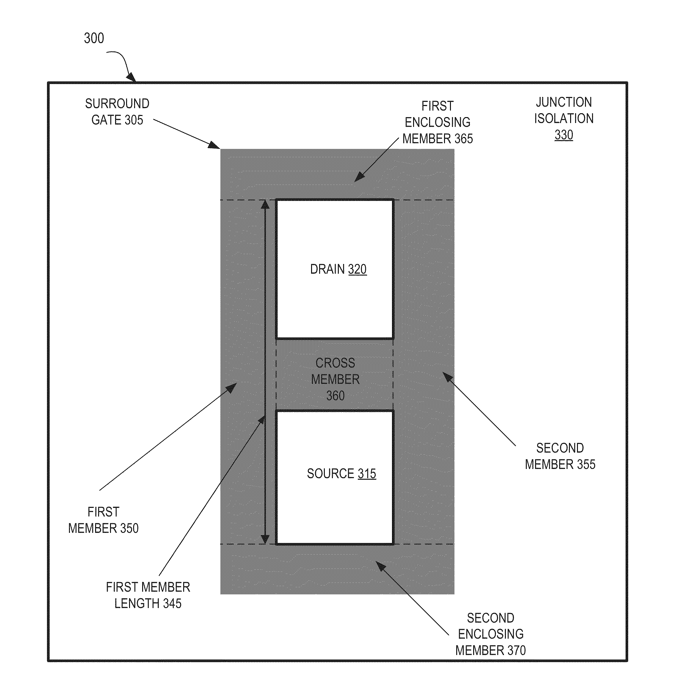
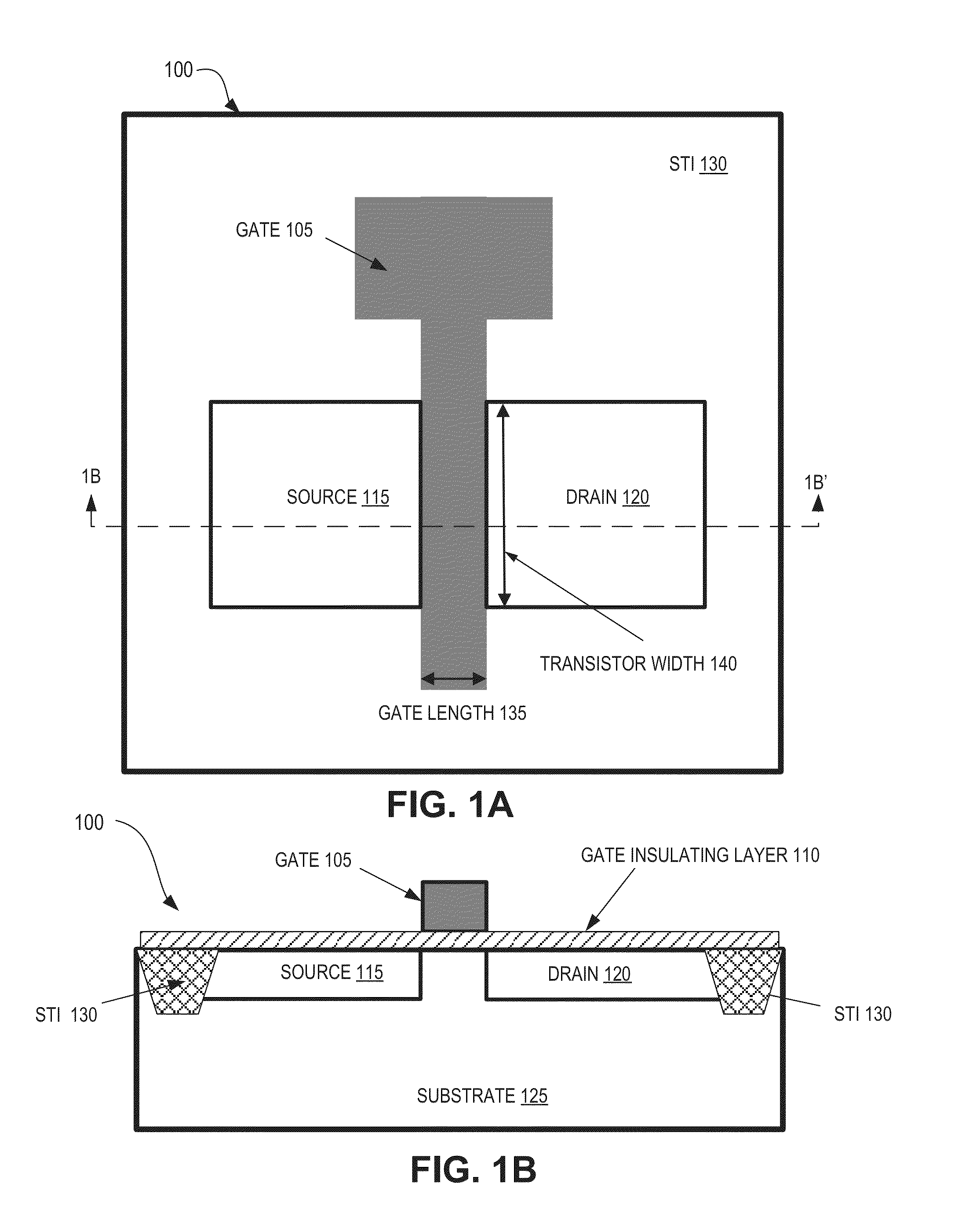
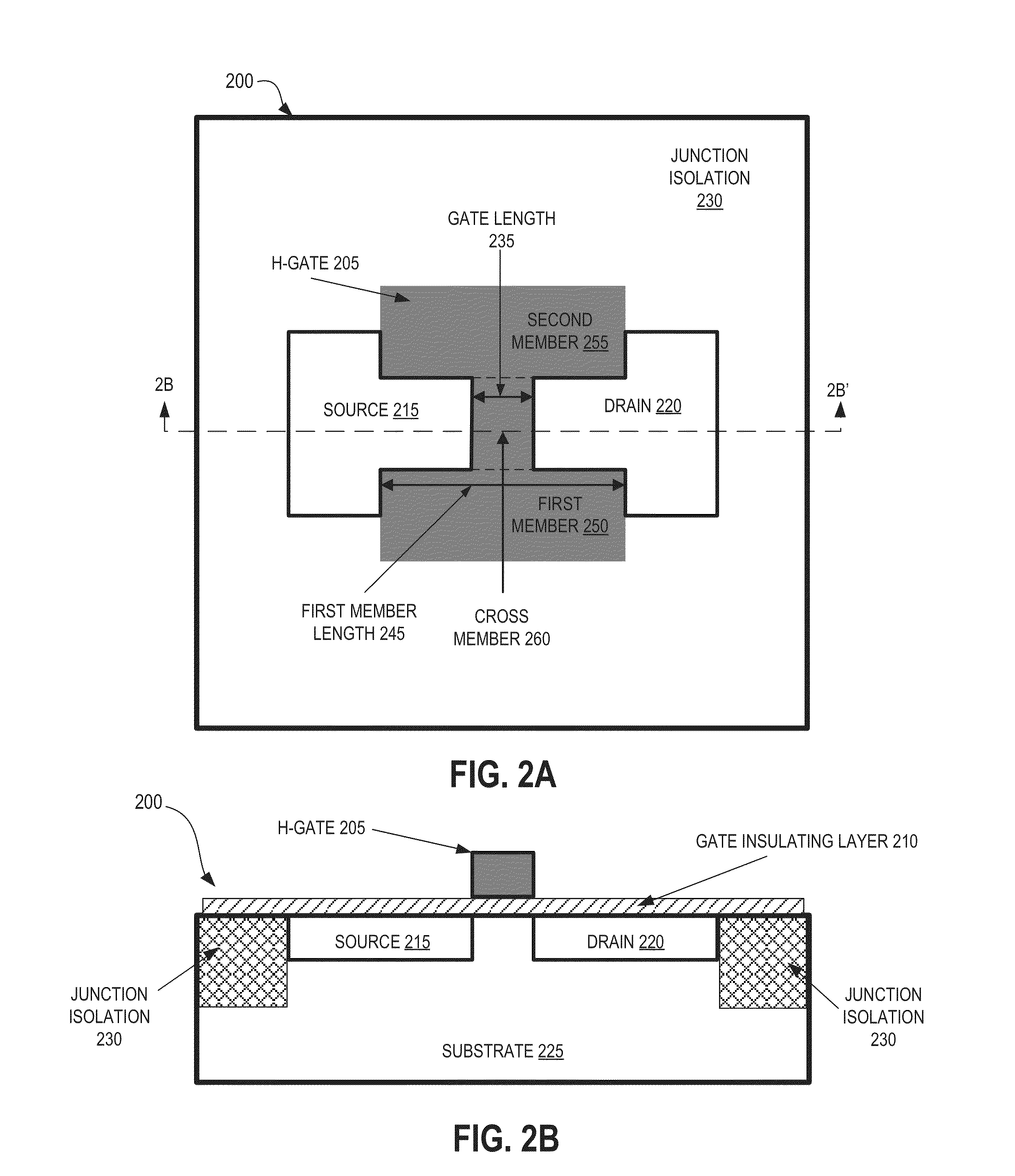
[0019]Embodiments of an apparatus and method of manufacture for a transistor are described herein. In the following description numerous specific details are set forth to provide a thorough understanding of the embodiments. One skilled in the relevant art will recognize, however, that the techniques described herein can be practiced without one or more of the specific details, or with other methods, components, materials, etc. In other instances, well-known structures, materials, or operations are not shown or described in detail to avoid obscuring certain aspects.

[0020]Reference throughout this specification to “one embodiment” or “an embodiment” means that a particular feature, structure, or characteristic described in connection with the embodiment is included in at least one embodiment of the present invention. Thus, the appearances of the phrases “in one embodiment” or “in an embodiment” in various places throughout this specification are not necessarily all referring to the sa...


PUM


Abstract

A device includes a transistor including a source and a drain disposed in a substrate and a gate disposed above the substrate. The gate includes a first longitudinal member disposed above the source and the drain and running substantially parallel to a channel of the transistor. The first longitudinal member is disposed over a first junction isolation area. The gate also includes a second longitudinal member disposed above the source and the drain and running substantially parallel to the channel of the transistor. The second longitudinal member is disposed over a second junction isolation region. The gate also includes a cross member running substantially perpendicular to the channel of the transistor and connecting the first longitudinal member to the second longitudinal member. The cross member is disposed above and between the source and the drain.

Description

TECHNICAL FIELD[0001]This disclosure relates generally to electronics, and in particular but not exclusively, relates to transistors.BACKGROUND INFORMATION[0002]Image sensors are widely used in digital still cameras, cellular phones, security cameras, as well as in, medical, automobile, and other applications. Complementary metal-oxide-semiconductor (“CMOS”) technology is used to manufacture lower cost image sensors on silicon substrates. In a large number of image sensors, the image sensor commonly includes hundreds, thousand or even millions of light sensor cells or pixels. A typical individual pixel includes a micro-lens, a filter, a photosensitive element, a floating diffusion region, and one or more transistors for reading out a signal from the photosensitive element. As image sensor pixels become smaller and smaller, the transistors inside them must also become smaller. However, conventional transistor technologies encounter isolation challenges and increased manufacturing exp...

Claims


Application Information

Patent Timeline
Patent Type & Authority Applications(United States)
IPC IPC(8): H01L31/113H01L21/336
CPCH01L27/14614H01L27/14627H01L27/14643H01L29/0847H01L29/6659H01L21/761H01L29/0692H01L29/4238
Inventor LYU, JEONG-HOMANABE, SOHEI
Owner OMNIVISION TECH INC
Why Eureka
Try Eureka