Woven mesh substrate with semiconductor elements, and method and device for manufacturing the same

a technology of semiconductor elements and woven mesh, which is applied in the direction of weaving, looms, yarns, etc., can solve the problems of high defect ratio of solar battery modules, inability to test the functioning and danger of spherical semiconductor elements being torn away, so as to reduce the number of components and reduce the manufacturing cost. , the effect of reducing the number of components

Inactive Publication Date: 2013-06-13
SPHELAR POWER
View PDF0 Cites 26 Cited by
  • Summary
  • Abstract
  • Description
  • Claims
  • Application Information

AI Technical Summary

Benefits of technology

[0027]And, according to the manufacturing device, apart from fundamentally obtaining similar advantageous effects described above, the following further beneficial effects are also obtained. Since it is possible to additionally provide an application mechanism and a semiconductor element supply mechanism while taking effective advantage of a supply side guidance roller, a peddle mechanism, and a reed mechanism of an already existing weaving machine, accordingly this is advantageous from the point of view of design, manufacture, and manufacturing cost of a manufacturing device for a woven mesh substrate with attached semiconductor elements, and it is possible to produce a manufacturing device for automatically manufacturing a woven mesh substrate with attached semiconductor elements.
[0028]And since, according to the invention of claim 16, with this woven mesh substrate with attached semiconductor elements, along with the plurality of spherical semiconductor elements being grouped into a plurality of groups by taking row direction element groups that consist of a plurality of spherical semiconductor elements arranged along the horizontal direction as units, and the plurality of row direction element groups being arranged in a plurality of rows, also the conductive connection members that consist of one or a plurality of horizontal strands are disposed between adjacent ones of the row direction element groups, and the plurality of spherical semiconductor elements in each of the row direction element groups are electrically connected in parallel via a pair of the conductive connection members, and the plurality of row direction element groups are connected in series via the plurality of conductive connection members, accordingly, in the case of a woven mesh substrate with attached semiconductor elements for light reception, it is possible to set the voltage of the electricity that is generated freely via the number of series connections, and also it is possible to set the current of the electricity that is generated freely via the number of parallel connections.
[0029]And since, in the case of a woven mesh substrate with semiconductor elements for light reception, the plurality of spherical semiconductor elements are connected in series in the vertical direction and also are connected in parallel in the horizontal direction, accordingly, even if it happens that some portion becomes partially shaded, it is possible to ensure that the influence that is exerted on the output of the other portion of the spherical semiconductor elements that is not shaded is still kept to the minimum limit.
[0030]Moreover, this woven mesh substrate with semiconductor elements is capable of light reception or light emission with equal efficiency from both its sides, both top and bottom. This woven mesh substrate with semiconductor elements is an intermediate manufactured product, that is flexible, light in weight, thin, bendable, see through, and translucent to daylight, and it can be finished into various types of final manufactured product, according to the application.
[0031]Furthermore, since it is not necessary to provide any separate conducting lines for series connection to the series connection construction of this woven mesh substrate with semiconductor elements, accordingly it is possible to reduce the number of components, so that it is possible to reduce the manufacturing cost. And, since it is possible to arrange the spherical semiconductor elements more closely together without providing any unnecessary gaps between the element groups, accordingly it is possible to enhance the tensile strength and the bending strength (resistance), while also being able to enhance the light reception performance or the light emission performance.
[0032]In addition to above described manufacturing method, it would also be acceptable to arrange to employ various additional steps of the following types.

Problems solved by technology

However, when tension is applied in the direction of series connection, the spherical semiconductor elements receive this tension directly, so that there is a danger of the spherical semiconductor elements being torn away.
However, with the manufacturing method of Patent Document #4, since the formation of the electrodes and establishment of the electrical connections between the mesh like structural material and the spherical semiconductor elements are performed simultaneously, accordingly there is the problem that testing for checking the functioning of the spherical semiconductor elements is not possible, because the pushing of the spherical semiconductor elements into the meshes of the mesh like structural material is not performed subsequently to formation of their electrodes.
For this reason, even if faulty spherical semiconductor elements are mixed in with the others, this fact cannot be detected, and therefore the defect ratio of the solar battery module becomes high.
Furthermore, with the finished solar battery module, since the spherical semiconductor elements project on one of its surfaces, accordingly light from the rear surface of the solar battery module cannot be effectively utilized, and the light reception sensitivity for light that is incident from the rear surface becomes low, which is undesirable.
Moreover, since the flexibility of the solar battery module when the module is mechanically bent is not symmetrical between its two sides but is biased towards one side, accordingly the convenience of use becomes bad.

Method used


Image

  • Woven mesh substrate with semiconductor elements, and method and device for manufacturing the same
  • Woven mesh substrate with semiconductor elements, and method and device for manufacturing the same
  • Woven mesh substrate with semiconductor elements, and method and device for manufacturing the same

Examples


embodiment 1

[0080]First, the woven mesh substrate with semiconductor elements 1 of the present invention will be explained.

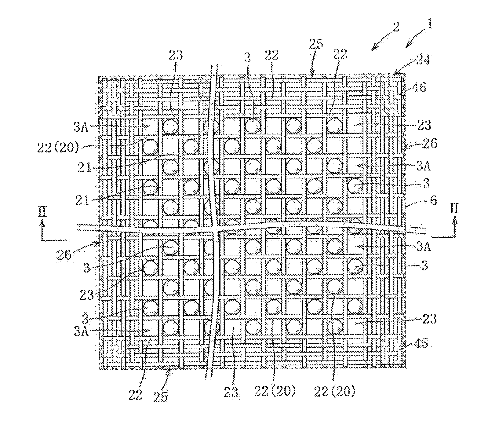
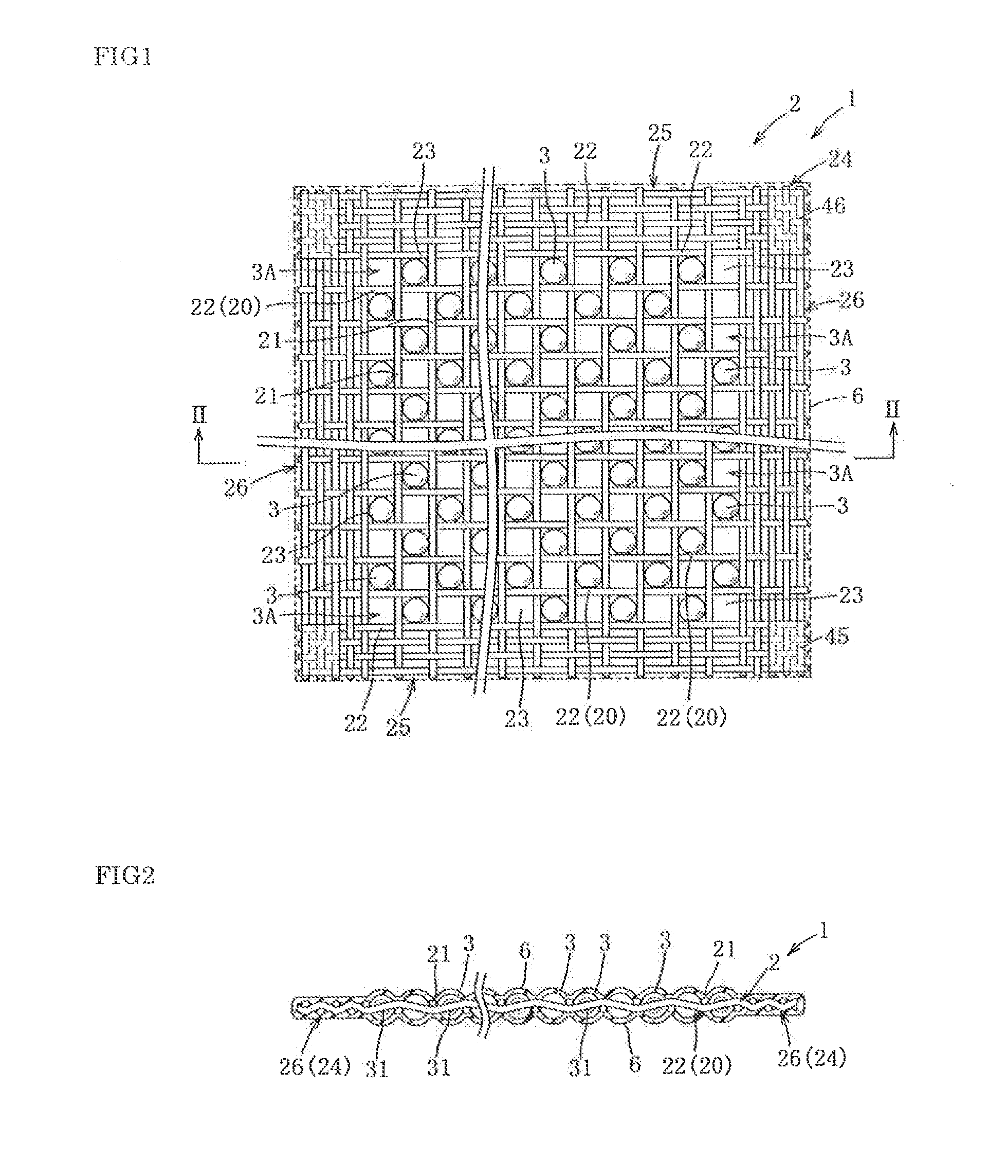
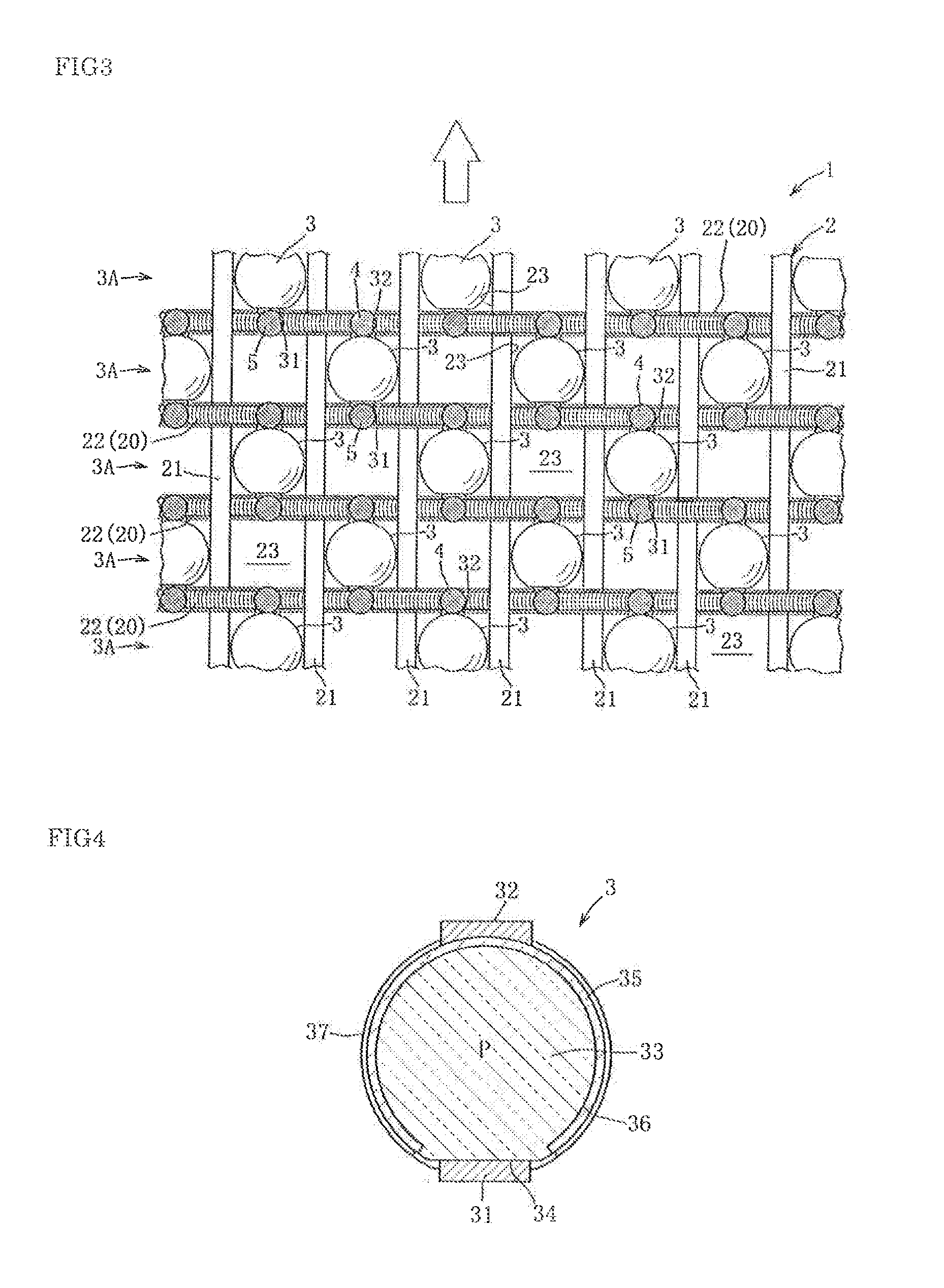
[0081]As shown in FIGS. 1 through 3, the woven mesh substrate with semiconductor elements 1 (hereinafter termed the “woven mesh substrate with elements 1”) comprises: a woven mesh substrate 2 that is formed as a net having meshes 23 in matrix form arranged in a plurality of rows and a plurality of columns, and woven from a plurality of vertical strands 21 that are insulating and a plurality of horizontal strands 22 that are conductive; a plurality of spherical solar cells 3 (which correspond to spherical semiconductor elements) that are installed to the plurality of meshes 23 of the woven mesh substrate 2; and a plurality of first and second conducting junction materials 4, 5 for connecting these spherical solar cells 3 to the horizontal strands 22 (i.e. to conductive connection members 20). Protective insulating layers 6 are formed on both the sides of the woven mesh subst...

embodiment 2

[0164]While, in this embodiment, there are described a woven mesh substrate with semiconductor elements 1A in which the woven mesh substrate with semiconductor elements 1 of the above Embodiment #1 is partially altered, and a manufacturing device 50A for manufacturing this woven mesh substrate with semiconductor elements 1A in which the manufacturing device 50 described above is partially altered and a manufacturing method for the woven mesh substrate with semiconductor elements 1A, to constitutional elements that are similar to elements of the first embodiment the same reference numerals will be appended, and explanation thereof will be omitted, with only those elements that are different being explained.

[0165]First, the woven mesh substrate with semiconductor elements 1A will be explained. As shown in FIGS. 9 and 10, the woven mesh substrate with attached semiconductor elements 1A (hereinafter “woven mesh substrate with elements 1A”) is a device that produces a similar woven mesh ...

embodiment 3

[0174]While, in this embodiment, a manufacturing device 50B is described in which the manufacturing devices 50, 50A described above for manufacturing the woven mesh substrates with elements 1, 1A are partially altered, to constitutional elements that are similar to elements of the first and second embodiments the same reference numerals will be appended, and explanation thereof will be omitted, with only those elements that are different being explained. It should be understood that while, with the manufacturing devices 50, 50A of the first and second embodiments described above, the woven mesh substrates with elements 1, 1A were woven while being pulled out in the horizontal direction, with the manufacturing device 50B of this embodiment, the woven mesh substrate with elements 1, 1A is woven while being pulled out downwards.

[0175]First, the manufacturing device 50B will be explained.

[0176]As shown in FIGS. 13 and 14, the manufacturing device 50B is substantially the manufacturing d...


PUM

PropertyMeasurementUnit
lengthaaaaaaaaaa
diameteraaaaaaaaaa
diameteraaaaaaaaaa

Abstract

A woven mesh substrate with semiconductor elements and a method and a device for manufacturing such a substrate, and more particularly a technique that makes it possible to exploit a woven mesh substrate with semiconductor elements in which a plurality of spherical semiconductor elements having a light receiving function or a light-emitting function are installed on a woven mesh substrate in net form that is made up from a plurality of vertical strands that are insulating and a plurality of horizontal strands that are conductive.

Description

TECHNICAL FIELD[0001]The present invention relates to a woven mesh substrate with semiconductor elements and to a method and a device for manufacturing such a substrate, and more particularly relates to a technique that makes it possible to exploit a woven mesh substrate with semiconductor elements in which a plurality of spherical semiconductor elements having a light-receiving function or a light-emitting function are installed on a woven mesh substrate in net form that is made up from a plurality of vertical strands that are insulating and a plurality of horizontal strands that are conductive.BACKGROUND TECHNOLOGY[0002]From the past, development has been underway of light reception devices such as solar batteries and so on, and of light emission devices such as EL displays and so on, having a construction in which a thin layer of semiconductor is formed over a flexible sheet that is insulating or conductive. While such semiconductor devices, over the whole range from small to com...

Claims


Application Information

Patent Timeline
Patent Type & Authority Applications(United States)
IPC IPC(8): H01L21/02
CPCD03D1/0076Y10T29/41D10B2401/20H01L25/0753H01L31/035281H01L31/048H01L31/0508H01L31/068H01L33/20H01L33/24H01L33/505H01L21/02Y02E10/547D03D9/00D03D13/008D03D15/0011D03D15/0027D03J1/00D03J1/06D10B2101/06D10B2101/12D10B2101/20H01L2924/1017H01L2224/16245D10B2401/16D03D1/0088D02G3/441D03D15/267D03D15/47H01L31/042H01L33/00D03D1/00D03D41/00
Inventor NAKATA, JOSUKE
Owner SPHELAR POWER
Why Eureka
Try Eureka