Method for manufacturing damascene structure

a damascene and structure technology, applied in the direction of semiconductor/solid-state device manufacturing, basic electric elements, electric apparatus, etc., can solve the problems of inferior evenness of the planarized surface and dishing, and achieve superior evenness, avoid dishing problems, and improve the effect of cmp results

Active Publication Date: 2013-07-18
UNITED MICROELECTRONICS CORP
View PDF77 Cites 8 Cited by
  • Summary
  • Abstract
  • Description
  • Claims
  • Application Information

AI Technical Summary

Benefits of technology

The present invention provides methods for manufacturing a damascene structure that can improve the CMP result and obtain a surface of superior evenness without rendering any adverse impact to the final products. This is achieved by forming dummy via holes in the substrate to average the pattern densities on the surface and avoid dishing problem. After the dual damascene structure is formed, the dummy via holes are removed, and no impact is rendered to subsequent processes. The method can also position dummy via holes in a dummy-blocking region and remove them by the CMP process without affecting the final products.

Problems solved by technology

For example, when a surface being polished includes patterns having different pattern densities, the planarization rates of the CMP are different based upon respective pattern densities, and thus evenness of the planarized surface is inferior, and even suffers dishing problem.

Method used


Image

  • Method for manufacturing damascene structure
  • Method for manufacturing damascene structure
  • Method for manufacturing damascene structure

Examples


Embodiment Construction

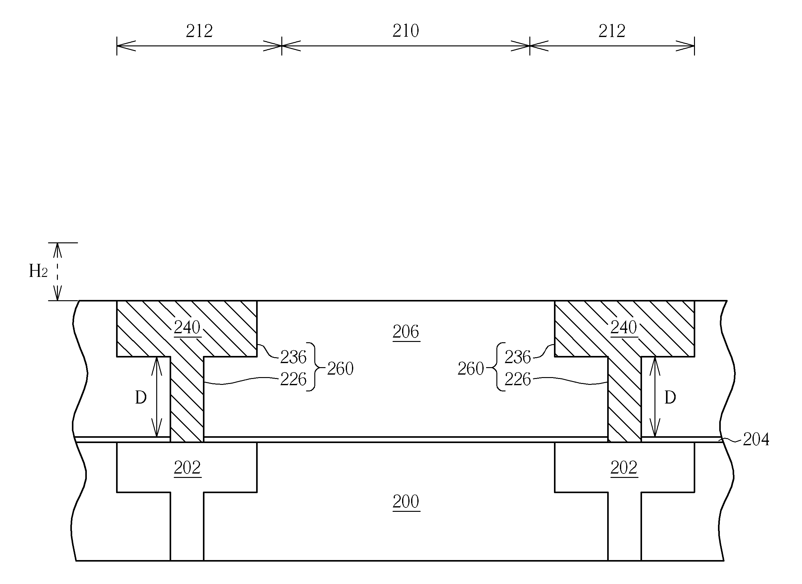
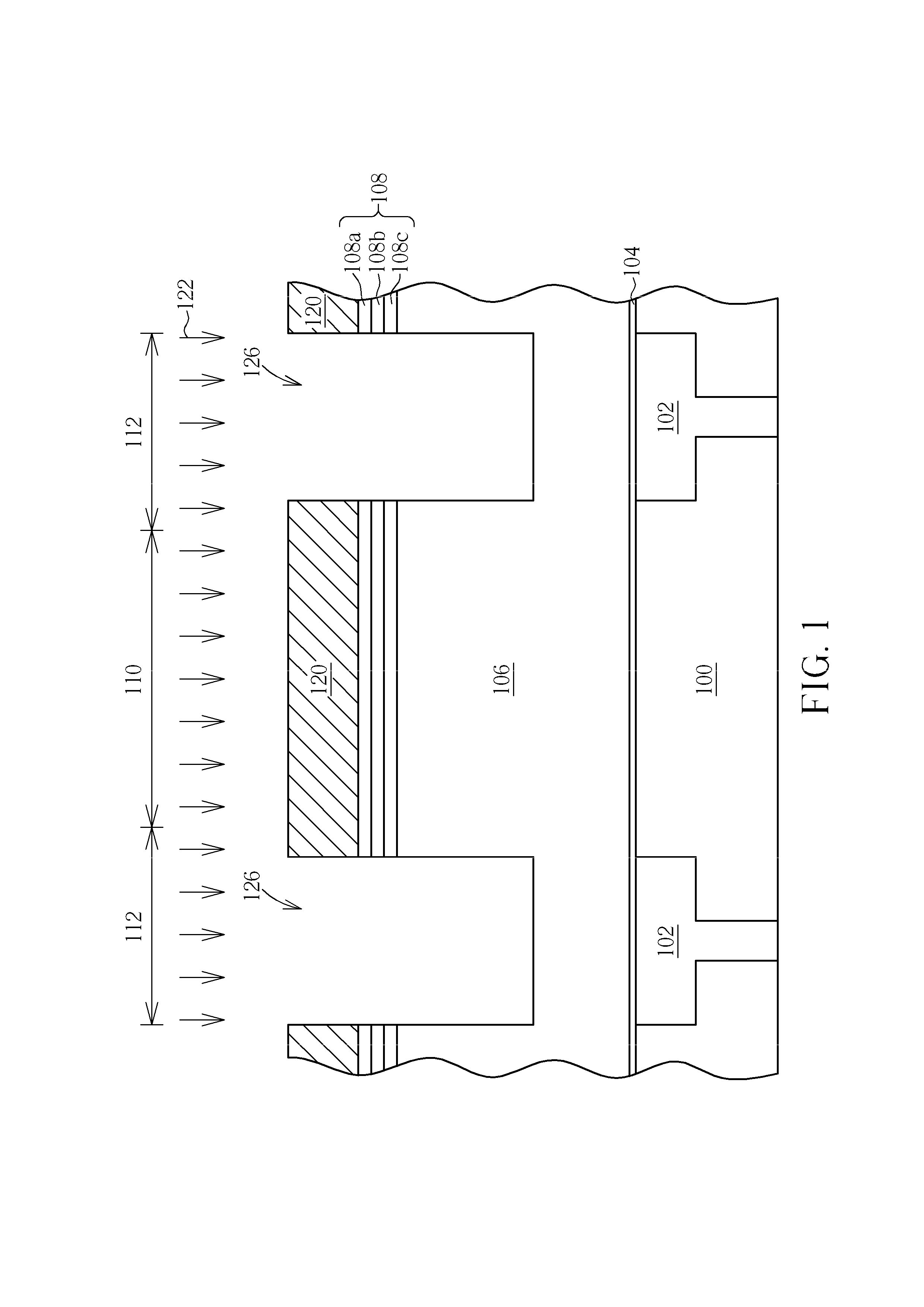
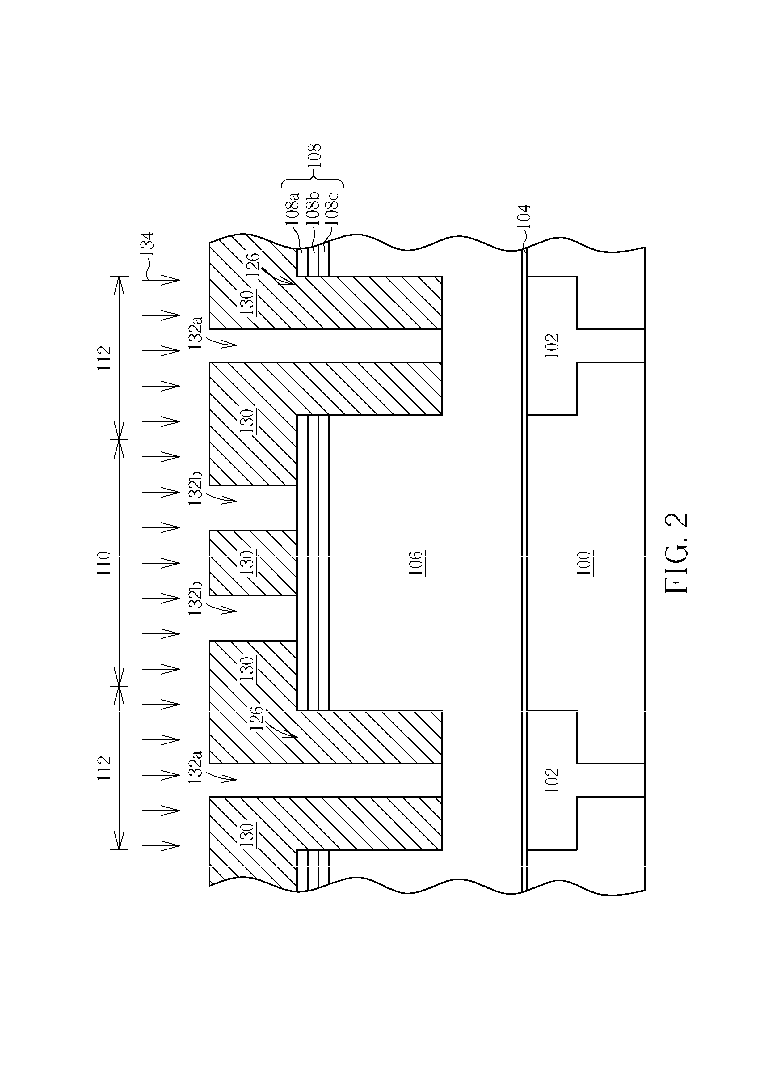
[0020]Please refer to FIGS. 1-5, which are schematic drawings illustrating a method for manufacturing a damascene structure provided by a first preferred embodiment of the present invention. As shown in FIG. 1, the preferred embodiment first provides a substrate 100, for example but not limited to a silicon substrate, a silicon-containing substrate, or a silicon-on-insulator (SOI) substrate. It is noteworthy that the substrate 100 includes at least a dummy-blocking region 110 and element regions 112 defined thereon according to the preferred embodiment. The dummy-blocking region 110 is a particularly defined region where dummy elements are not allowed to exist within a product such as micro electro mechanical systems (MEMS). The substrate 100 further includes a conductive layer 102 formed therein, and a base layer 104 covering the conductive layer 102 formed thereon. In the preferred embodiment, the conductive layer 102 includes conductive elements such as a wire, a doped region, or...


PUM


Abstract

A method for manufacturing a damascene structure includes providing a substrate having a dielectric layer formed thereon, forming at least a trench in the dielectric layer, forming at least a via hole and a dummy via hole in the dielectric layer, forming a first conductive layer filling up the trench, the via hole and the dummy via hole on the substrate, and performing a chemical mechanical polishing process to form a damascene structure and simultaneously to remove the dummy via hole.

Description

BACKGROUND OF THE INVENTION[0001]1. Field of the Invention[0002]The present invention relates generally to a method for manufacturing a damascene structure, and more particularly, to a method for manufacturing a damascene structure capable of improving chemical mechanical polishing (hereinafter abbreviated as CMP) result.[0003]2. Description of the Prior Art[0004]In the fabrication of semiconductor integrated circuits (ICs), semiconductor devices are generally connected by several metallic interconnecting layers commonly referred to as multi-level interconnects, and damascene process has been deemed a convenient and predominant method for forming the multi-level interconnects. Principally, the damascene process includes etching a dielectric material layer to form trench and / or via patterns, filling the patterns with conductive materials such as copper, and performing a planarization process. Thus a metal interconnect is obtained.[0005]Those skilled in the art have well known that th...

Claims


Application Information

Patent Timeline
Patent Type & Authority Applications(United States)
IPC IPC(8): H01L21/768
CPCH01L21/76813H01L21/76807
Inventor LIOU, EN-CHIUANYANG, CHIH-WEIHUANG, CHIH-SENHU, CHAN-YUANFU, SSU-I
Owner UNITED MICROELECTRONICS CORP
Why Eureka
Try Eureka