Dummy patterns and method for generating dummy patterns

Active Publication Date: 2012-11-22
UNITED MICROELECTRONICS CORP
View PDF4 Cites 12 Cited by
  • Summary
  • Abstract
  • Description
  • Claims
  • Application Information

AI Technical Summary

Benefits of technology

[0010]According to the dummy patterns and the method for generating dummy patterns provided by the present invention, the first dummy patterns having the second density corresponding to the first density of the layout pattern is formed in the layout region for preliminarily equalizing the pattern densities in the layout region. Then, the layout region is divided into the sub-regions for checking sub-region by sub-region and thus the third density of each sub-region is obtained. Thereafter, the size of the first dummy patterns in each sub-region is adjusted according the difference between the third density and the second density. Therefore the pattern densities in each sub-region are further precisely adjusted. In other words, by adjusting the size of the first dummy pattern in each sub-region, the pattern densities, which are originally different from each other, of the sub-regions are smartly adjusted and equalized. Accordingly, the sub-regions obtaining equalized densities are beneficial to the CMP process and improve the CMP result.

Problems solved by technology

Besides the thickness variation problem, the uneven surface after CMP process further suffers serious problems such as pattern size error and poor critical size uniformity (CDU).
Furthermore, it is found that different pattern densities also adversely impact other semiconductor process such as patterning process or etching process.
Though the dummy patterns alleviate density difference between the low pattern density regions and the high pattern density regions, it is no longer competent when the wafer or the chip is formed to have more regions with varied densities due to the complexity of the integrated circuit (IC) design.
Furthermore, the conventional dummy patterns also suffer from several drawbacks and limitations such as being irresistible to stress between regions with different pattern densities and increases optical proximity correction (OPC) processing time.

Method used


Image

  • Dummy patterns and method for generating dummy patterns
  • Dummy patterns and method for generating dummy patterns
  • Dummy patterns and method for generating dummy patterns

Examples


Embodiment Construction

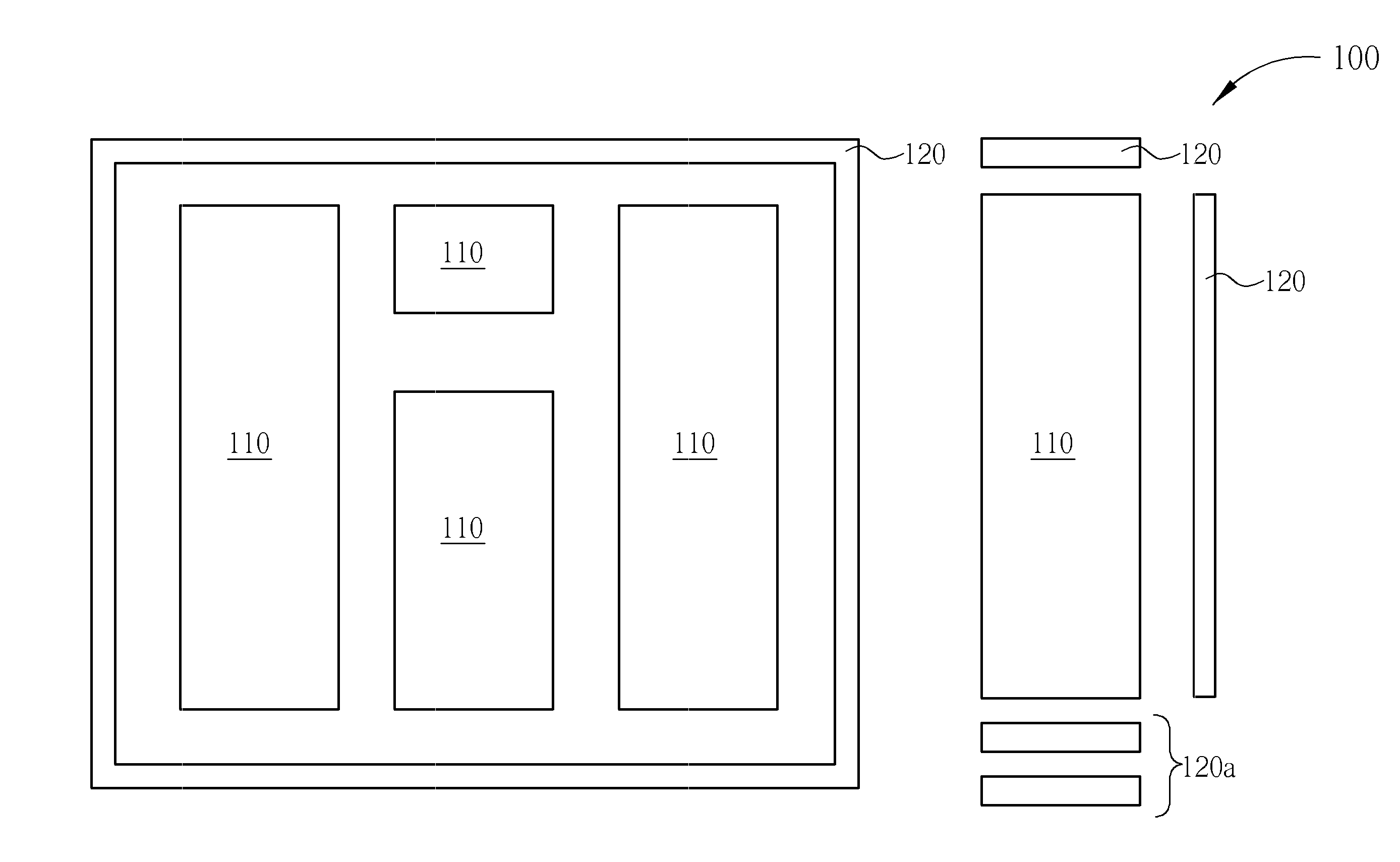
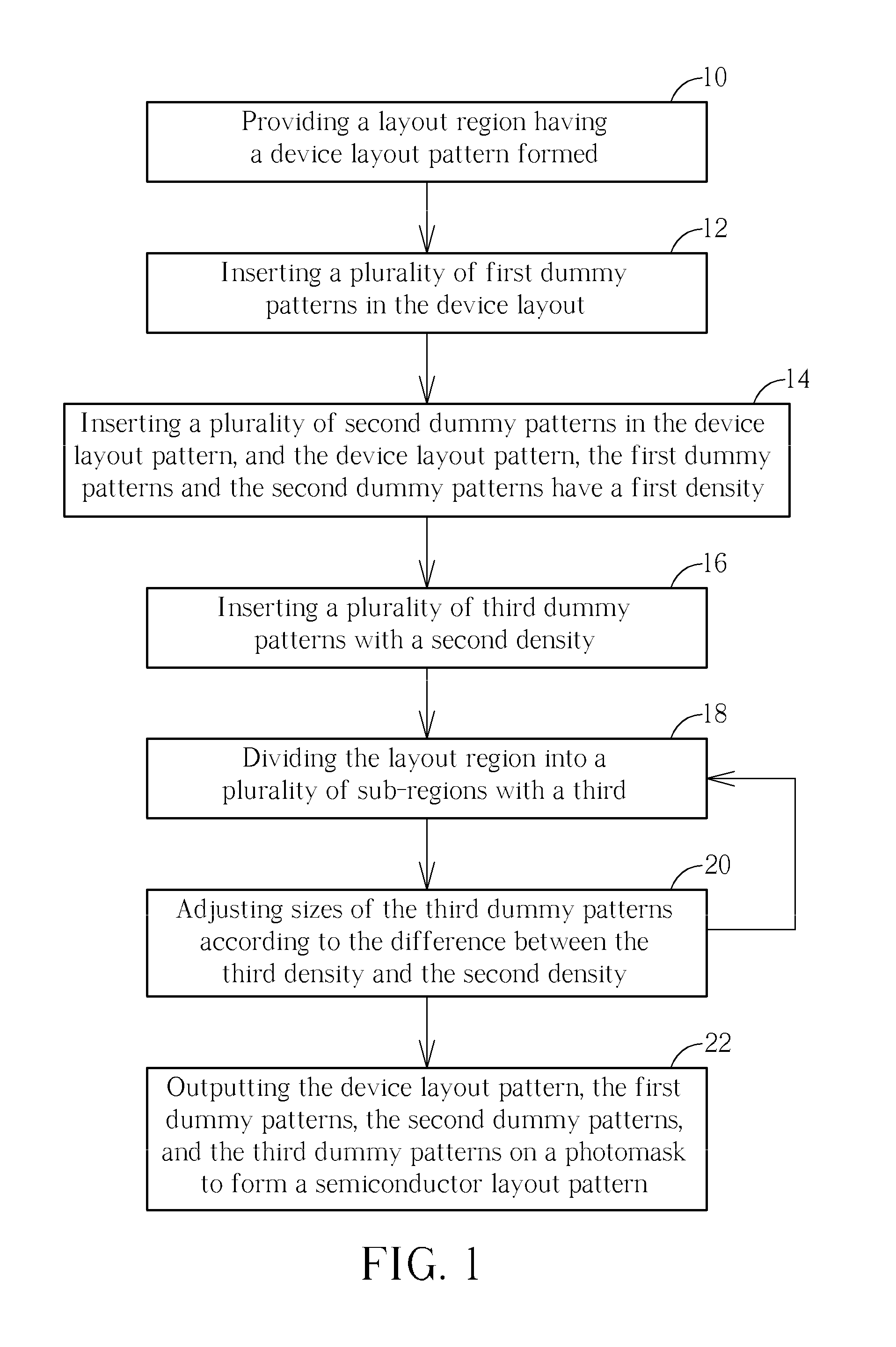
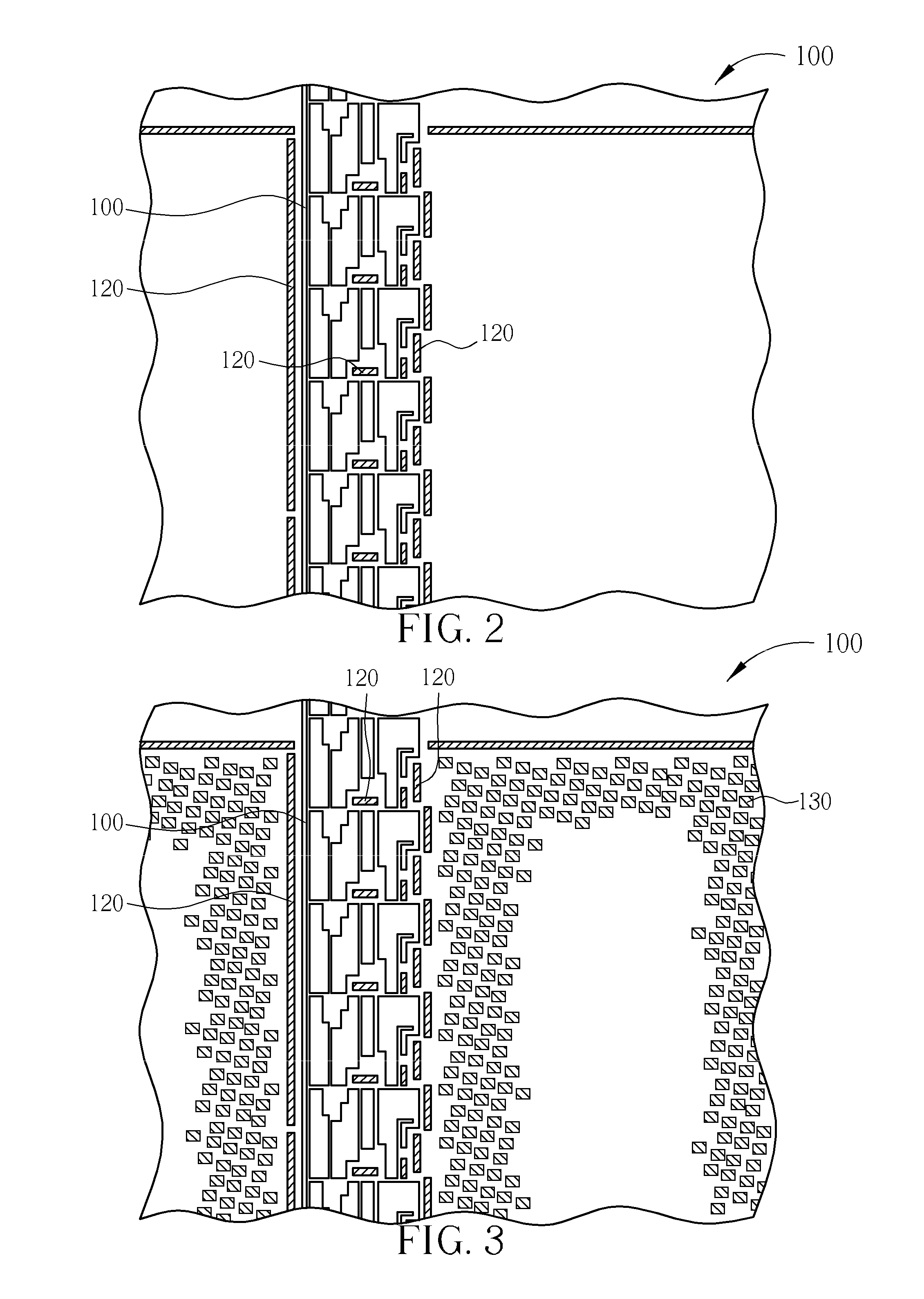
[0015]Please refer to FIGS. 1-8, wherein FIG. 1 is a flowchart illustrating a method for generating dummy patterns according to a first preferred embodiment of the present invention, FIGS. 2-8 are drawings illustrating the method for generating dummy patterns according to the first preferred embodiment, and FIG. 5 is an enlarged view of a portion of FIG. 4. As shown in FIG. 1 and FIG. 2, the preferred embodiment first performs:

[0016]Step 10: Providing a Layout Region Having a Device Layout Pattern Formed Therein

[0017]It is well-known to those skilled in the art that an original circuit layout patterns designed by the circuit design engineer is outputted on a photomask, and then transferred to an object layer by photolithography and etching processes for producing a product that satisfies the electrical function of the original circuit design. In the preferred embodiment, the layout region 100 includes a region on a photomask that used to form layout patterns on an object layer, and ...


PUM


Abstract

A method for generating dummy patterns includes providing a layout region having a layout pattern with a first density, inserting a plurality of first dummy patterns with a second density corresponding to the first density in the layout pattern, dividing the layout region into a plurality of sub-regions with a third density, adjusting a size of the first dummy pattern according to a difference between the second density and the third density, and outputting the layout pattern and the first dummy patterns on a photomask.

Description

BACKGROUND OF THE INVENTION[0001]1. Field of the Invention[0002]The invention relates to dummy patterns and a method for generating dummy patterns, and more particularly, to dummy patterns and a method for generating dummy patterns used in planarization process.[0003]2. Description of the Prior Art[0004]Along with an increase in speed of semiconductor devices, downsizing and higher integration of elements, such as transistors and multilevel interconnects are now in progress. An ever increasing accuracy and precision for forming circuit layout with higher density on the wafer is therefore required. Of course, those of ordinary skill in the art will easily recognize that layout with higher density requires better surface flatness of the wafer for increasing the accuracy for forming the layout pattern. Conventionally, chemical mechanical polishing (CMP) process is an effective and important method for wafer planarization. And result of CMP becomes critical for forming necessary element...

Claims


Application Information

Patent Timeline
IPC IPC(8): G03F1/00G06F17/50
CPCG06F17/5072G06F2217/12H01L23/48H01L23/481H01L2924/0002G03F1/70H01L2924/00G06F30/392G06F2119/18Y02P90/02H01L21/0334H01L23/528
Inventor TSAI, CHEN-HUACHEN, JIAN-CHENGTSAI, CHIN-YUEHFAN, YAO-JENCHEN, HENG-KUNYANG, HSIANG
Owner UNITED MICROELECTRONICS CORP
Why Eureka
Try Eureka