Substrate transfer apparatus, substrate transfer method, and non-transitory storage medium

Active Publication Date: 2013-08-08
TOKYO ELECTRON LTD
View PDF1 Cites 9 Cited by
  • Summary
  • Abstract
  • Description
  • Claims
  • Application Information

AI Technical Summary

Benefits of technology

The invention aims to provide a technique that can accurately transfer a circular substrate with a cutout edge to a module using a small number of light source parts and light receiving parts. The light source part provides light to the light receiving part at each position with the substrate displaced, and the detection range of the sensor part is determined based on the amount of received light. When there is an overlap, the substrate position is further displaced and the edge of the substrate is detected, allowing for accurate delivery to the module. This technique reduces the number of required light source and light receiving parts.

Problems solved by technology

When a detection range of the detection part overlaps with the cutout, the position of the wafer at the holding part cannot be correctly detected any longer, and therefore, something needs to be done.
Further, in the case of failure of the plurality of detection parts due to some problem, it is conceivable that the transfer of the wafer under treatment in the apparatus is stopped and an operator enters the apparatus to collect the wafer and removes the wafer.
In this case, however, the treatment on the wafer is suspended in the apparatus and the throughput may greatly decrease.
H08-031905 and No. 2006-351884 in which these problems are not into consideration cannot solve the problems.

Method used


Image

  • Substrate transfer apparatus, substrate transfer method, and non-transitory storage medium
  • Substrate transfer apparatus, substrate transfer method, and non-transitory storage medium
  • Substrate transfer apparatus, substrate transfer method, and non-transitory storage medium

Examples


Embodiment Construction

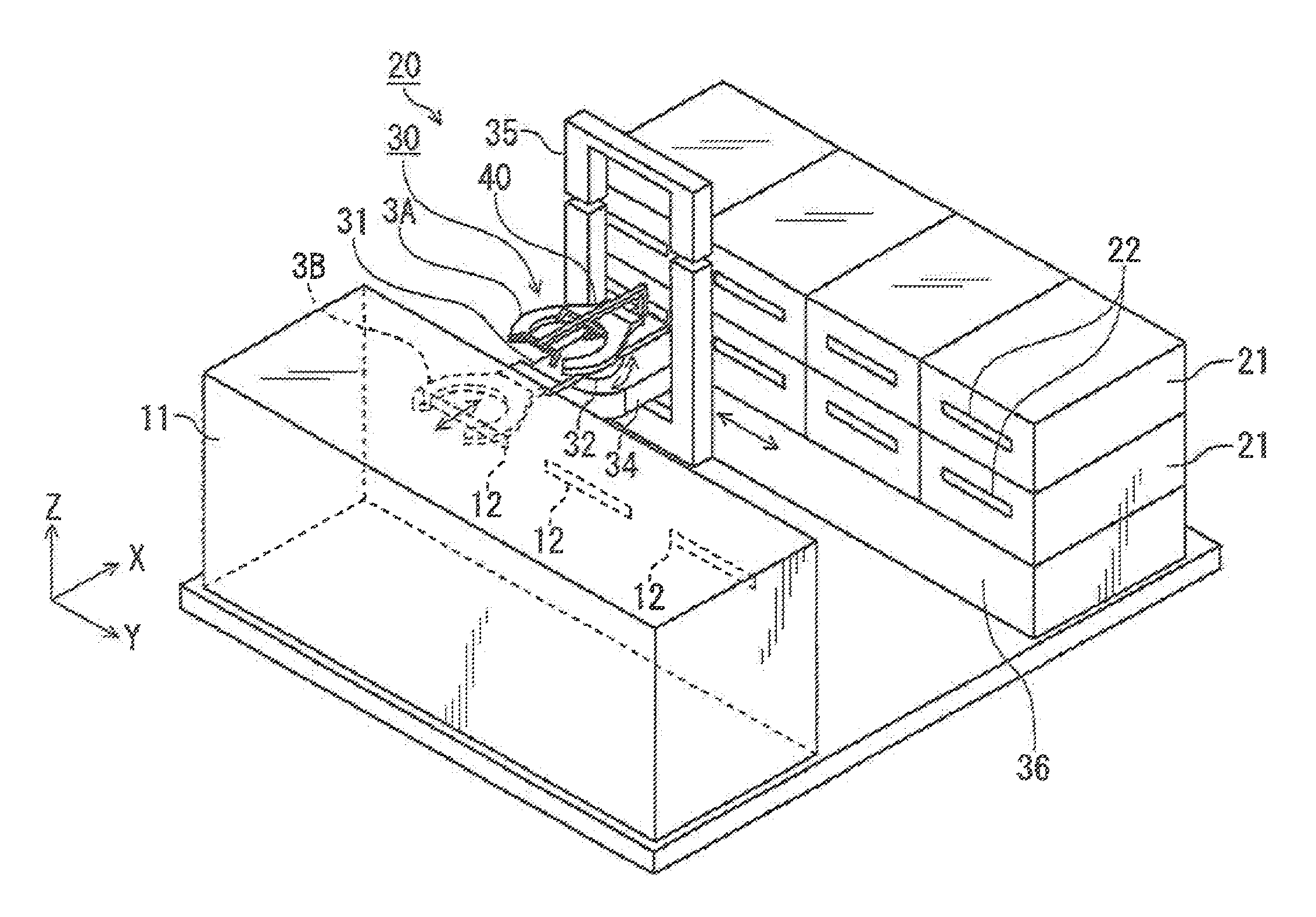
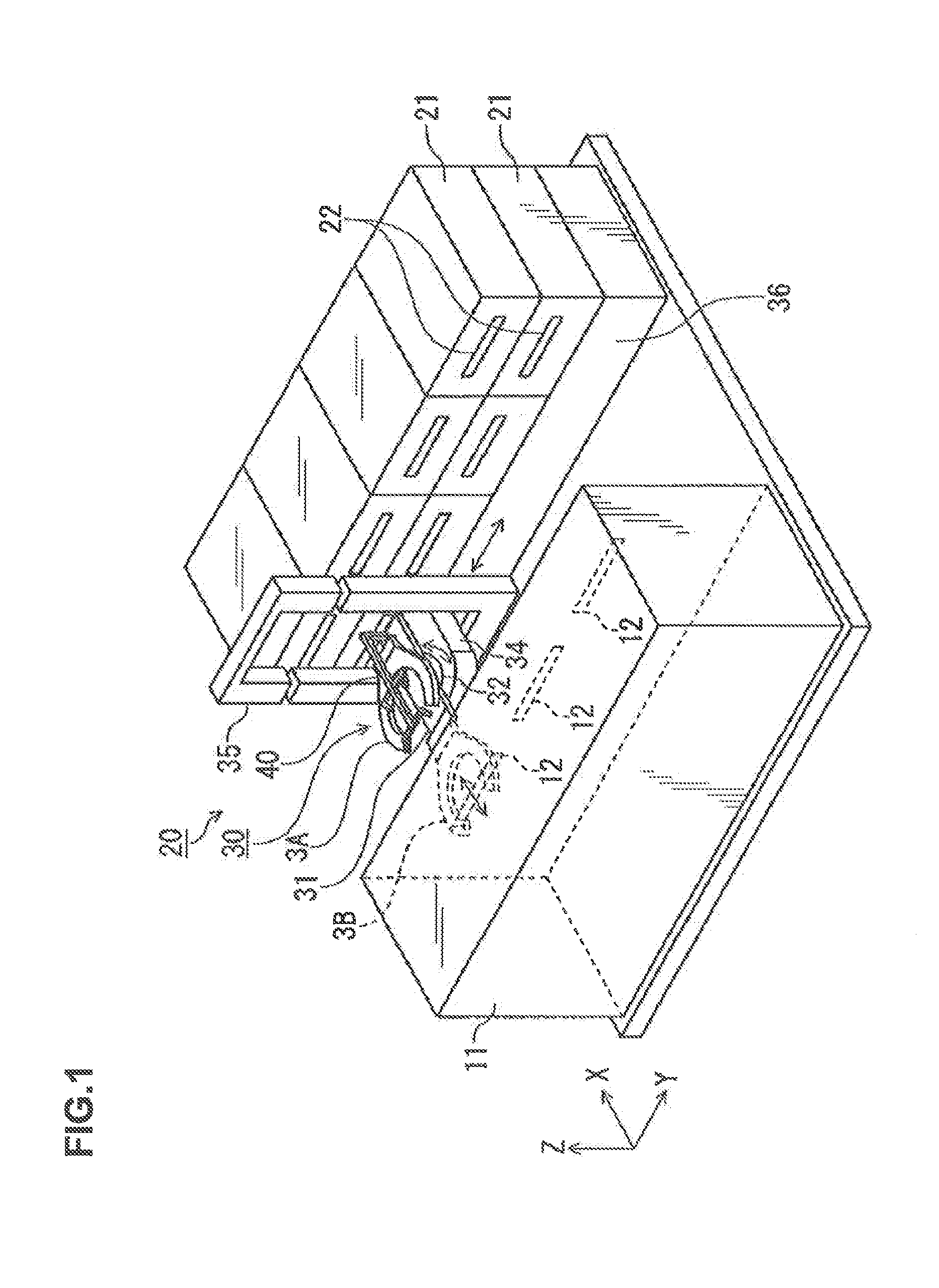
[0081]FIG. 1 illustrates a perspective view of a transfer arm 30 that forms a substrate transfer apparatus and a group of modules to which a wafer W that is a circular substrate is delivered by the transfer arm 30. An edge portion of the wafer W is provided with a notch N that is a cutout. A numeral 11 in the drawing denotes a housing that houses a module COT applying a resist to the wafer W. A wafer W is delivered to the module COT through a transfer port 12 and subjected to a resist coating treatment. The housing 11 faces a transfer path 20 for the wafer W in which the transfer arm 30 moves, and a plurality of heating modules 21 are provided to face the housing 11 across the transfer path 20. The heating module 21 includes a heating plate on which the wafer W coated with the resist is mounted, and performs a heat treatment on the wafer W. A numeral 22 in the drawing denotes a transfer port for the wafer W in the heating module 21.

[0082]The transfer arm 30 transfers the wafer W fro...


PUM


Abstract

A substrate transfer apparatus to transfer a circular substrate provided with a cutout at an edge portion thereof, includes: a sensor part including three light source parts applying light to positions different from one another at the edge portion, and three light receiving parts paired with the light source parts; and a drive part for moving the substrate holding part, wherein the three light source parts apply light to the light receiving parts so that whether or not a detection range of the sensor part overlaps with the cutout of the substrate is determined on the basis of an amount of received light by each light receiving part, and when it is determined that there is an overlap at any position, positions of the edge portion of the substrate are further detected with the position of the substrate displaced with respect to the sensor part.

Description

CROSS REFERENCE TO RELATED APPLICATION[0001]The present application is related to, claims priority from and incorporates by reference Japanese Patent Applications No. 2012-022047 filed on Feb. 3, 2012.BACKGROUND OF THE INVENTION[0002]1. Field of the Invention[0003]The present invention relates to a substrate transfer apparatus for transferring a substrate between modules, a substrate transfer method, and a non-transitory storage medium storing a program for executing the substrate transfer method.[0004]2. Description of the Related Art[0005]In a manufacturing process of, for example, a semiconductor device, a plurality of treatment modules each performing treatment on a wafer being a substrate are provided in an apparatus and the wafer is sequentially transferred by a substrate transfer apparatus between the treatment modules, whereby predetermined treatments are performed. The substrate transfer apparatus includes a holding part holding the wafer.[0006]For performing appropriate tr...

Claims


Application Information

Patent Timeline
IPC IPC(8): G05D3/12
CPCH01L21/67259G05D3/125H01L21/681H01L21/67742H01L21/68714H01L21/68757G05B19/4189G05B2219/45032G05B2219/45051
Inventor HAYASHI, TOKUTAROUDOUKI, YUICHIMAEJIMA, HIROMITSU
Owner TOKYO ELECTRON LTD
Why Eureka
Try Eureka