Transfer method, mounting method, transfer device, and mounting device

Active Publication Date: 2019-07-18
TORAY ENG CO LTD
View PDF0 Cites 11 Cited by
  • Summary
  • Abstract
  • Description
  • Claims
  • Application Information

AI Technical Summary

Benefits of technology

The present invention aims to solve the issue of air resistance when transferring LED chips during mounting. The method includes a transfer device and mounting device that can accurately transfer and mount LED chips while eliminating the influence of air resistance. This results in better accuracy and efficiency in the transfer process.

Problems solved by technology

However, a problem with the technique described in Patent Literature 1 was that the LED chips may be displaced due to the influence of air resistance when transferring the LED chips to the transfer substrates.

Method used


Image

  • Transfer method, mounting method, transfer device, and mounting device
  • Transfer method, mounting method, transfer device, and mounting device
  • Transfer method, mounting method, transfer device, and mounting device

Examples


first embodiment

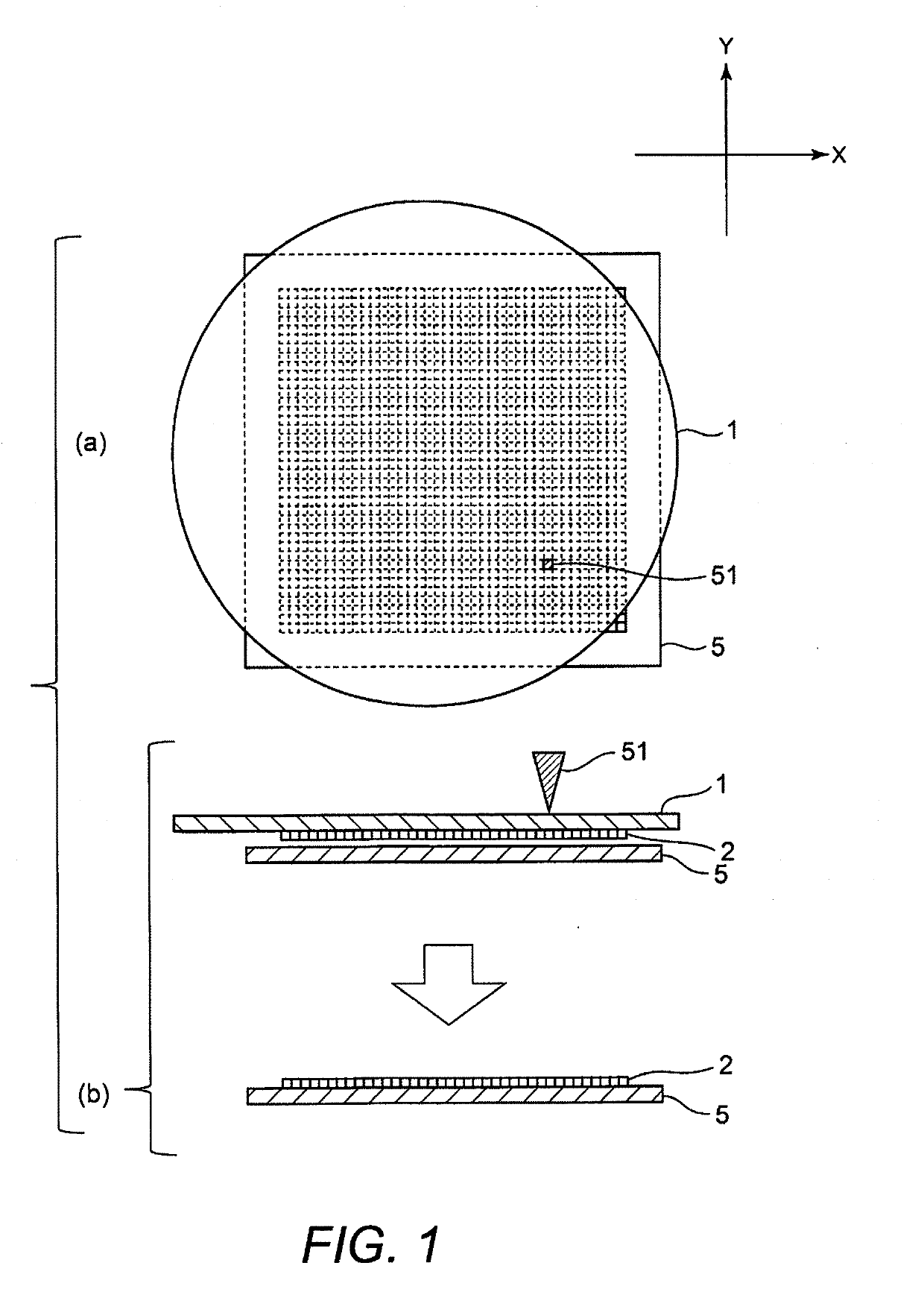
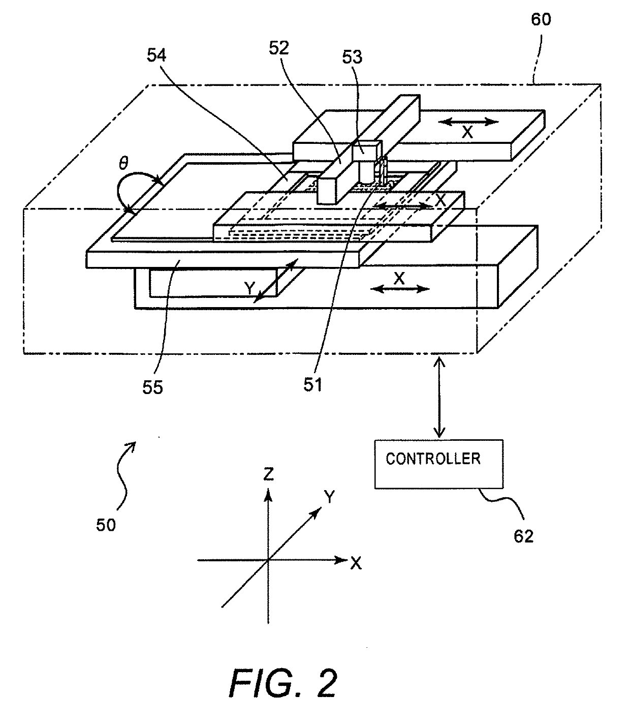
[0044]A first embodiment of the present invention will be described with reference to FIGS. 1 and 2. FIG. 1 is a diagram illustrating a transfer method in the first embodiment of the present invention. FIG. 2 is a diagram illustrating a transfer device in the first embodiment of the present invention.

[0045]Transfer Method

[0046]As shown in part (a) of FIG. 1, the first surface side of the LED chips 2 is grown a from a carrier substrate 1 made of sapphire, and the second surface, which is the surface on the opposite side from the first surface, is exposed to the outside and has bumps formed on it. The carrier substrate 1 has a circular or quadrangular shape, and may be composed of gallium arsenide besides sapphire. The LED chips 2 are diced into a plurality of units (from several hundred to tens of thousands) and arranged two-dimensionally on the carrier substrate 1. Small LED chips 2, called a micro LEDs, measure 50×50 μm or less, and are arranged at a pitch obtained by adding the di...

second embodiment

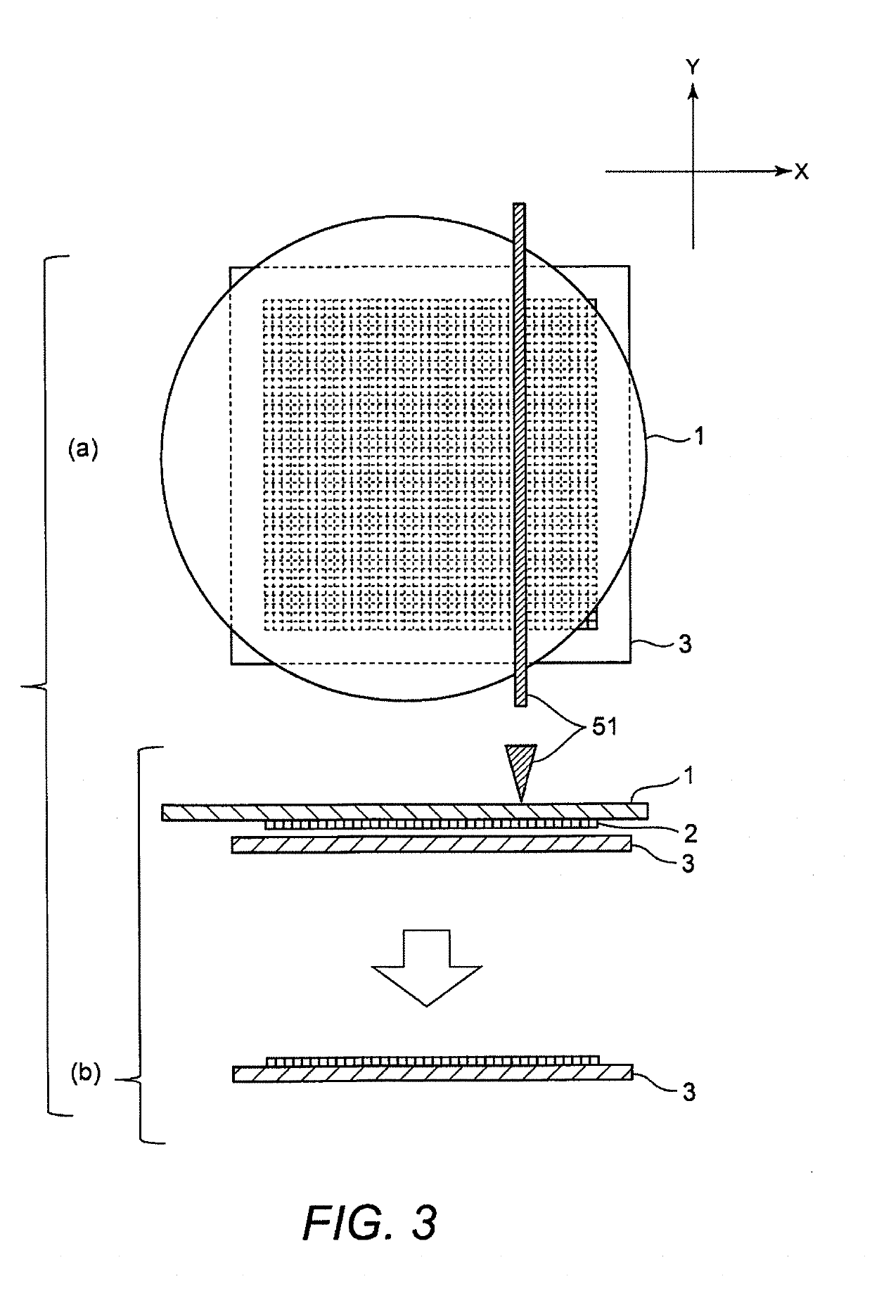
[0071]A second embodiment differs from the first embodiment in that the LED chips 2 held on the carrier substrate are mounted at high speed to a circuit board. The mounting method according to the second embodiment of the present invention will be described with reference to FIGS. 3 to 9. FIG. 3 is a diagram illustrating a first transfer step of the mounting method in the second embodiment of the present invention. FIG. 4 is a diagram illustrating a second transfer step of the mounting method in the second embodiment of the present invention. FIG. 5 is a diagram illustrating the beginning of a first mounting step of the mounting method in the second embodiment of the present invention. FIG. 6 is a diagram illustrating the middle of the first mounting step of the mounting method in the second embodiment of the present invention. FIG. 7 is a diagram illustrating the end of the first mounting step of the mounting method in the second embodiment of the present invention. FIG. 8 is a dia...

third embodiment

[0126]In a third embodiment of the present invention, the first transfer step is different from that in the second embodiment. The mounting method in the third embodiment of the present invention will be described with reference to FIG. 10. FIG. 10 is a diagram illustrating the first transfer step of the mounting method in the third embodiment of the present invention.

[0127]In the first transfer step in the third embodiment, first, the second surface of the LED chips 2, the first surface of which is held by the carrier substrate 1, is transferred by being stuck onto an adhesive layer (not shown) on the surface of the first transfer substrate 3. Next, as shown in part (a) of FIG. 10, the opposite side of the carrier substrate 1 from the side holding the LED chips 2 is subjected to back grinding with a grinder 56. That is, the carrier substrate 1 is removed by scraping it off of the opposite side from the side where the LED chips 2 are provided. Particularly in the case of red LEDs, l...


PUM


Abstract

A transfer method for transferring LED chips, a first surface of which is held on a transfer substrate, on a transfer-target substrate is provided that comprises disposing the transfer-target substrate such that the transfer-target substrate faces, across a gap, a second surface of the LED chips on an opposite side from the first surface of the LED chips, and transferring the LED chips on the transfer-target substrate by irradiating the transfer substrate with a laser light to separate the LED chips from the transfer substrate and by urging the LED chips toward the transfer-target substrate. At least the transferring of the LED chips to the transfer-target substrate being executed in a vacuum environment.

Description

[0001]This application is a continuation application of PCT International Application No. PCT / JP2017 / 033809 filed on Sep. 20, 2017, which claims priority to Japanese Patent Application Nos. 2016-190507 filed on Sep. 29, 2016 and 2017-009029 filed on Jan. 21, 2017. The entire disclosures of PCT International Application No. PCT / JP2017 / 033809 and Japanese Patent Application Nos. 2016-190507 and 2017-009029 are hereby incorporated herein by reference.BACKGROUNDField of the Invention[0002]The present invention relates to a transfer method, a mounting method, a transfer device, and a mounting device for transferring and mounting LED chips.Background Information[0003]In order to reduce the cost, LED chips have been made smaller, and efforts have been made to mount these smaller LED chips quickly and accurately. In particular, LEDs used for displays need for LED chips of 50×50 μm or smaller (called micro LEDs) to be mounted at high speed at an accuracy of just a few microns.[0004]Japanese ...

Claims


Application Information

Patent Timeline
IPC IPC(8): H01L21/683H01L25/075H01L33/62H01L23/00
CPCH01L21/6835H01L25/0753H01L33/62H01L24/16H01L24/81H01L2224/16225H01L2221/68354H01L2221/68368H01L2221/68381H01L2924/12041H01L2933/0066H01L2224/81203H01L2221/68327H01L2221/6834H01L33/0095H01L2224/16227H01L2224/75252H01L2224/81191H01L2924/351H01L24/75H01L2224/11002B23K26/38H01L21/52H01L21/67092H01L21/67144H01L21/67721H01L21/78H01L24/89H01L33/00
Inventor ARAI, YOSHIYUKI
Owner TORAY ENG CO LTD
Why Eureka
Try Eureka