Radio frequency IC device and method of manufacturing the same

Active Publication Date: 2012-03-29
MURATA MFG CO LTD
View PDF6 Cites 7 Cited by
  • Summary
  • Abstract
  • Description
  • Claims
  • Application Information

AI Technical Summary

Benefits of technology

[0007]Preferred embodiments of the present invention provide a radio frequency IC device that prevents variations in the value of capacitive coupling between a radio frequency IC element and a radiation electrode and has good signal transmission efficiency, and also provide a method of manufacturing the radio frequency IC device.
[0010]In the radio frequency IC device, the radio frequency IC element and the radiation electrode are coupled via a capacitor having the capacitance value C1 and a capacitor having the capacitance value C2 which are connected in series between the radio frequency IC element and the radiation electrode. That is, C1 and C2 are connected in series on a transmission path of a radio frequency signal. Here, the relationship between C1 and C2 is C1<C2. In this case, the total capacitance value C between the radio frequency IC element and the radiation electrode is controlled by the capacitance value C1 that is the smaller one. The capacitance value C1 is obtained between the input / output electrode included in the radio frequency IC element and the intermediate electrode included in the first base. The radio frequency IC element can be accurately mounted on the first base using an IC installation apparatus in the related art, and variations in the capacitance value C1 rarely occur. On the other hand, the capacitance value C2 is obtained between the intermediate electrode and the radiation electrode. Even if the first base is inaccurately mounted on the second base and variations in the capacitance value C2 occur, the capacitance value C2 has little effect on the capacitance value C between the radio frequency IC element and the radiation electrode. Accordingly, the occurrence of variations in the capacitance value C between the radio frequency IC element and the radiation electrode is suppressed and minimized, and the reduction in signal transmission efficiency can be prevented.
[0011]According to preferred embodiments of the present invention, variations in the value of capacitive coupling between a radio frequency IC element and a radiation electrode can be prevented, signal emission / reception performed by the radiation electrode becomes stable, and signal transmission efficiency is not reduced.

Problems solved by technology

However, in this radio frequency IC device, high accuracy is required when bonding these flexible sheets.
As a result, signal emission / reception performed by the radiation plate becomes unstable and signal transmission efficiency is reduced.

Method used


Image

  • Radio frequency IC device and method of manufacturing the same
  • Radio frequency IC device and method of manufacturing the same
  • Radio frequency IC device and method of manufacturing the same

Examples


first preferred embodiment

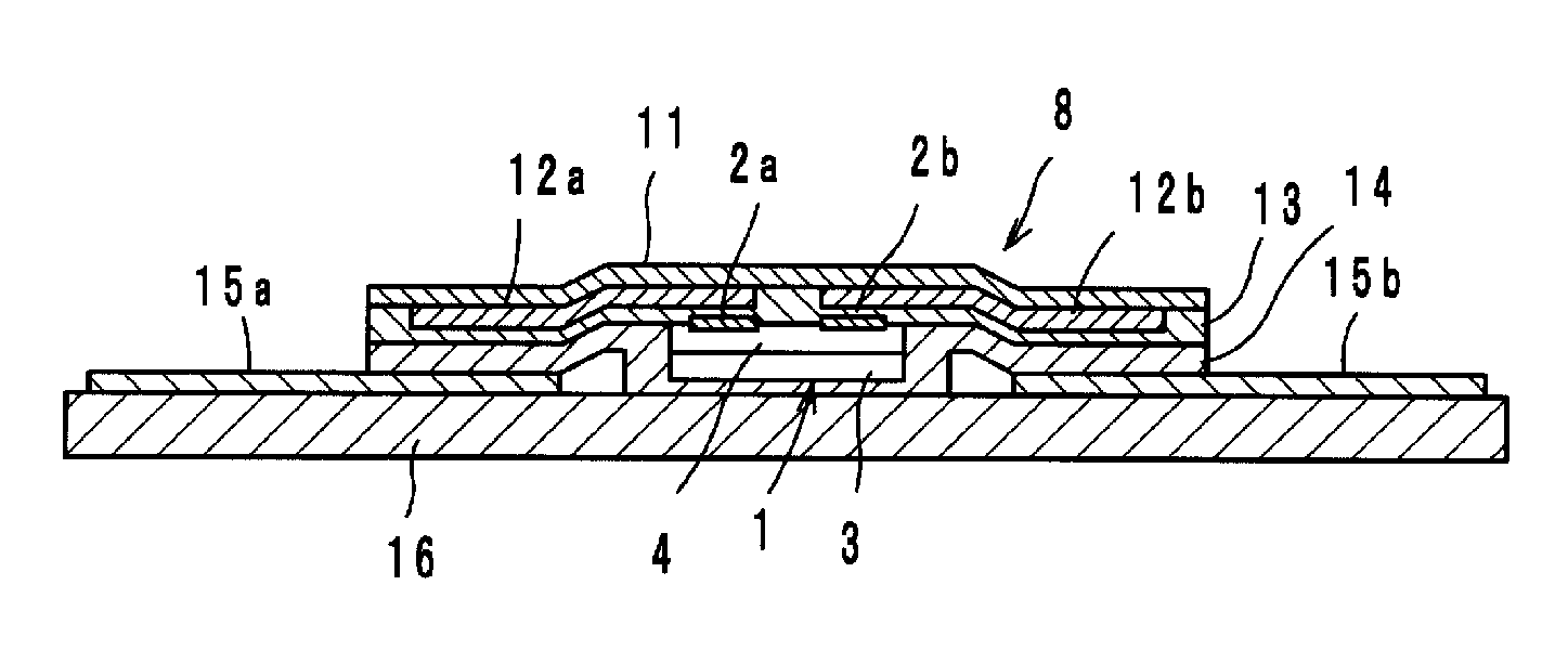
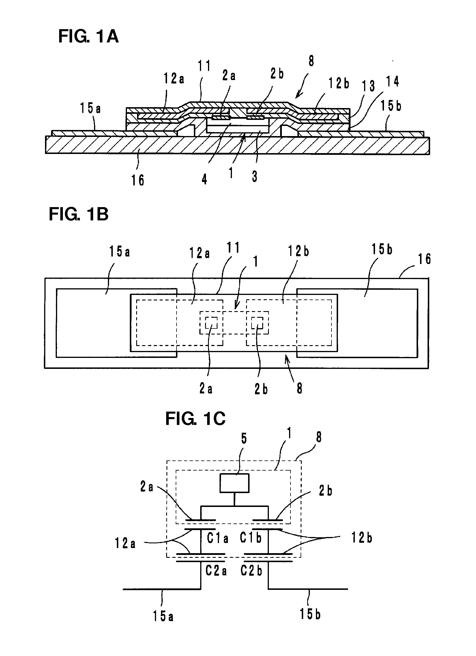
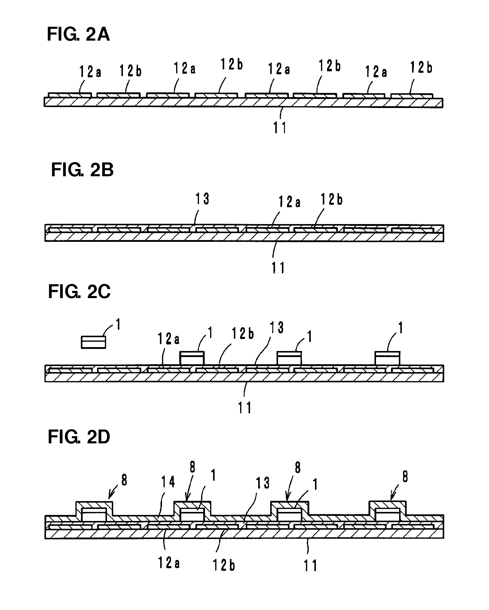
[0029]As illustrated in FIGS. 1A and 1B, a radio frequency IC device according to the first preferred embodiment includes a radio frequency IC element 1 obtained by mounting a radio frequency IC chip 5 (see FIG. 4) on a feeding circuit board 4 and covering the radio frequency IC chip 5 with a resin layer 3, a first base 11 including intermediate electrodes 12a and 12b, and a second base 16 including radiation electrodes 15a and 15b.

[0030]As illustrated in FIG. 4, the radio frequency IC chip 5 is connected to a feeding circuit (not illustrated) in the feeding circuit board 4 via solder bumps 7, and input / output electrodes 2a and 2b are disposed on the surface of the feeding circuit board 4. The radio frequency IC element 1 is attached to the first base 11 via an insulating adhesive layer 13 so that the input / output electrodes 2a and 2b face the intermediate electrodes 12a and 12b, respectively. The input / output electrodes 2a and 2b are capacitively coupled to the intermediate electr...

second preferred embodiment

[0044]As illustrated in FIG. 7C, in a radio frequency IC device according to the second preferred embodiment, a single input / output electrode 22 is disposed on the surface of the feeding circuit board 4. The input / output electrode 22 faces and is capacitively coupled to an intermediate electrode 21. Except this point, the second preferred embodiment is preferably the same as the first preferred embodiment. FIG. 7B illustrates an equivalent circuit of a radio frequency IC device according to the second preferred embodiment. The input / output electrode 22 and the intermediate electrode 21 are capacitively coupled with the capacitance value C1. The capacitance value C1 is, for example, about 4 pF, and a capacitance value obtained by combining the capacitance value C2a between the intermediate electrode 21 and the radiation electrode 15a and the capacitance value C2b between the intermediate electrode 21 and the radiation electrode 15b is, for example, about 20 pF.

[0045]In the second pre...

third preferred embodiment

[0046]As illustrated in FIG. 8A, in a radio frequency IC device according to the third preferred embodiment, a single radiation electrode 30 is disposed on the second base 16. Like in the second preferred embodiment, the input / output electrode 22 is capacitively coupled to the intermediate electrode 21. FIG. 8B illustrates an equivalent circuit of a radio frequency IC device according to the third preferred embodiment. The input / output electrode 22 and the intermediate electrode 21 are capacitively coupled with the capacitance value C1, and the intermediate electrode 21 and the radiation electrode 30 are capacitively coupled with the capacitance value C2. The capacitance value C1 is, for example, about 3 pF, and the capacitance value C2 is, for example, about 20 pF.

[0047]In the third preferred embodiment, the radiation electrode 30 may have a large area (for use in the UHF frequency band), or have a loop shape (for use in the HF frequency band).


PUM

PropertyMeasurementUnit
Flexibilityaaaaaaaaaa
Efficiencyaaaaaaaaaa
Frequencyaaaaaaaaaa

Abstract

A radio frequency IC device that prevents variations in the value of capacitive coupling between a radio frequency IC element and a radiation electrode and has good signal transmission efficiency includes a radio frequency IC element including input / output electrodes and, a first base including intermediate electrodes that are capacitively coupled to the input / output electrodes and have capacitance values C1a and C1b, respectively, and a second base including radiation electrodes and that are capacitively coupled to the intermediate electrodes and have capacitance values C2a and C2b, respectively. A capacitance C1 obtained by combining C1a and C1b is smaller than a capacitance C2 obtained by combining C2a and C2b.

Description

BACKGROUND OF THE INVENTION[0001]1. Field of the Invention[0002]The present invention relates to radio frequency IC devices and methods of manufacturing the same, and, more particularly, to a radio frequency IC device preferably for use in an RFID (Radio Frequency Identification) system and a method of manufacturing the radio frequency IC device.[0003]2. Description of the Related Art[0004]In recent years, as a product management system, an RFID system has been developed in which a reader / writer for generating an induction field communicates with an IC tag (hereinafter referred to as a radio frequency IC device) attached to a product in a non-contact manner so as to obtain predetermined information stored in the IC tag. For example, Japanese Unexamined Patent Application Publication No. 2008-160874 discloses a radio frequency IC device used in an RFID system.[0005]In a radio frequency IC device disclosed in Japanese Unexamined Patent Application Publication No. 2008-160874 (for exam...

Claims


Application Information

Patent Timeline
IPC IPC(8): G06K19/077H05K13/04
CPCY10T29/4913G06K19/07756H01L2224/50
Inventor OSAMURA, MAKOTOKUBOTA, KENJIKATO, NOBORU
Owner MURATA MFG CO LTD
Why Eureka
Try Eureka