Waveguide structure

Pending Publication Date: 2021-12-09
SUBTRON TECH
View PDF3 Cites 0 Cited by
  • Summary
  • Abstract
  • Description
  • Claims
  • Application Information

AI Technical Summary

Benefits of technology

The patent text describes a waveguide structure that has a cavity filled with air to reduce energy loss during signal transmission. This structure has high average power handling and is not affected by dielectric materials outside the cavity. The technical effect of the design is to improve the performance of the waveguide structure during signal transmission.

Problems solved by technology

However, in the above structure, the dielectric material covered by the upper and lower metal surfaces and the copper pillar may lead to energy loss during signal transmission.
Particularly, when the frequency increases, such loss increases.
Therefore, selection of dielectric materials is often limited by the dissipation factor (DF), and costs of circuit implementation are thereby increased.

Method used


Image

  • Waveguide structure
  • Waveguide structure
  • Waveguide structure

Examples


Embodiment Construction

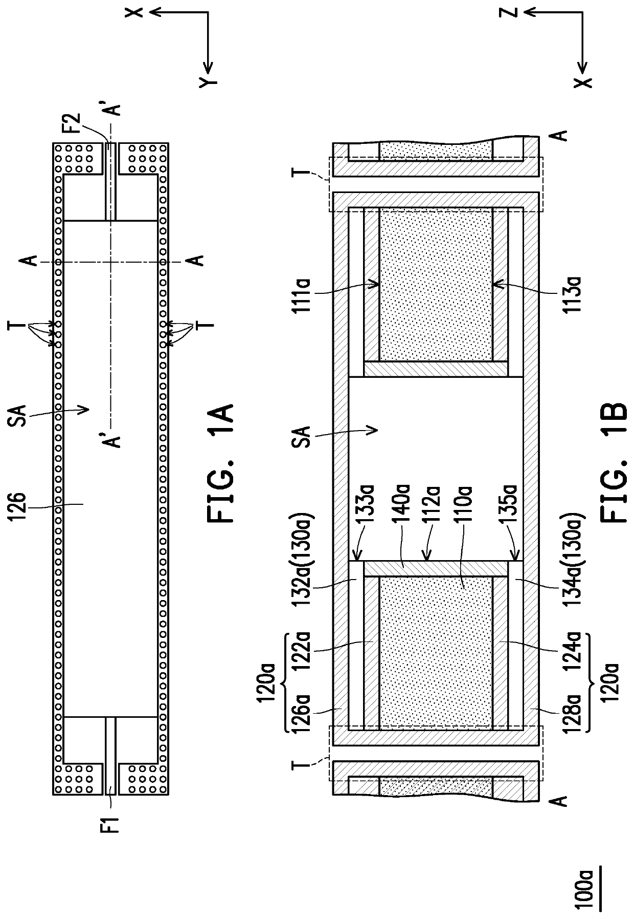
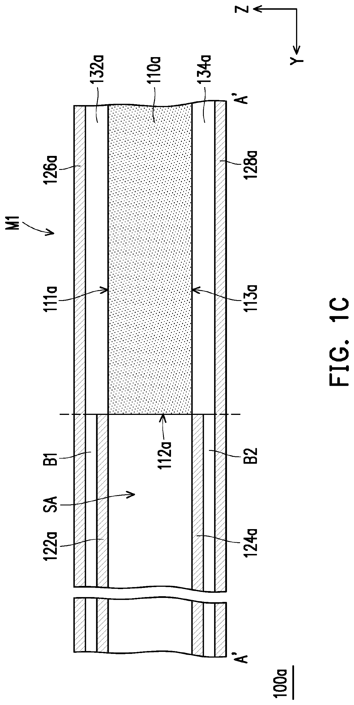
[0029]FIG. 1A is a schematic top view of a waveguide structure according to an embodiment of the disclosure. FIG. 1B is a schematic cross-sectional view taken along a line A-A in FIG. 1A. FIG. 1C is a schematic cross-sectional view taken along a line A′-A′ in FIG. 1A. Referring to FIG. 1A and FIG. 1B together, in the present embodiment, a waveguide structure 100a of the disclosure includes a dielectric layer 110a, a plurality of circuit layers 120a, a plurality of insulation layers 130a, and a conductor connection layer 140a. The dielectric layer 110a has an opening 112a. The circuit layers 120a are disposed on the dielectric layer 110a. The insulation layers 130a are alternately stacked with the circuit layers 120a. The conductor connection layer 140a covers an outer wall of the opening 112a in a direction perpendicular to the circuit layers 120a and connects at least two of the circuit layers 120a located on two opposite sides of the opening 112a. At least the conductor connection...


PUM


Abstract

A waveguide structure includes a dielectric layer, a plurality of circuit layers, a plurality of insulation layers, and a conductor connection layer. The dielectric layer has an opening. The circuit layers are disposed on the dielectric layer. The insulation layers and the circuit layers are alternately stacked. The conductor connection layer covers an outer wall of the opening in a direction perpendicular to the circuit layers and connects at least two circuit layers on two opposite sides of the opening. At least the conductor connection layer and a part of the circuit layers define an air cavity for transmitting signals at a position corresponding to the opening.

Description

CROSS-REFERENCE TO RELATED APPLICATION[0001]This application claims the priority benefit of Taiwan application serial no. 109118801, filed on Jun. 4, 2020. The entirety of the above-mentioned patent application is hereby incorporated by reference herein and made a part of this specification.BACKGROUND1. Technical Field[0002]The disclosure relates to a semiconductor structure, and in particular, to a waveguide structure.2. Description of Related Art[0003]At present, substrate integrated waveguide (SIW) structures are used in high-frequency circuits most of the time. In a cross-sectional view, the SIW consists of a dielectric material, upper and lower metal surfaces located on two opposite surfaces of the dielectric material, and a copper pillar penetrating through the dielectric material and connecting the upper and lower metal surfaces. However, in the above structure, the dielectric material covered by the upper and lower metal surfaces and the copper pillar may lead to energy loss...

Claims


Application Information

Patent Timeline
IPC IPC(8): H01Q1/38H01Q1/50H01P1/207H01P3/12
CPCH01Q1/38H01P3/121H01P1/207H01Q1/50H01P3/12H01P3/18H01P5/028H01P1/2088H01Q9/0457
Inventor TARNG, JENN-HWANLIU, NAI-CHENLIN, YIN-KAILEE, TSUNG-HANCHANG, CHAO-WEI
Owner SUBTRON TECH
Why Eureka
Try Eureka