Acoustic wave element and acoustic wave device using same
- Summary
- Abstract
- Description
- Claims
- Application Information
AI Technical Summary
Benefits of technology
Problems solved by technology
Method used
Image

Examples
first embodiment
(Configuration and Method of Production of SAW Element)
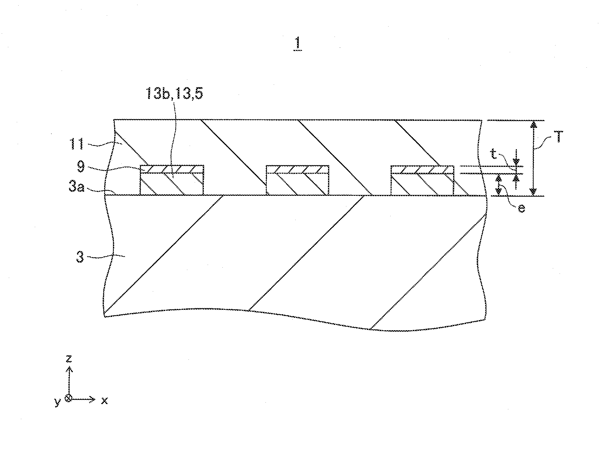
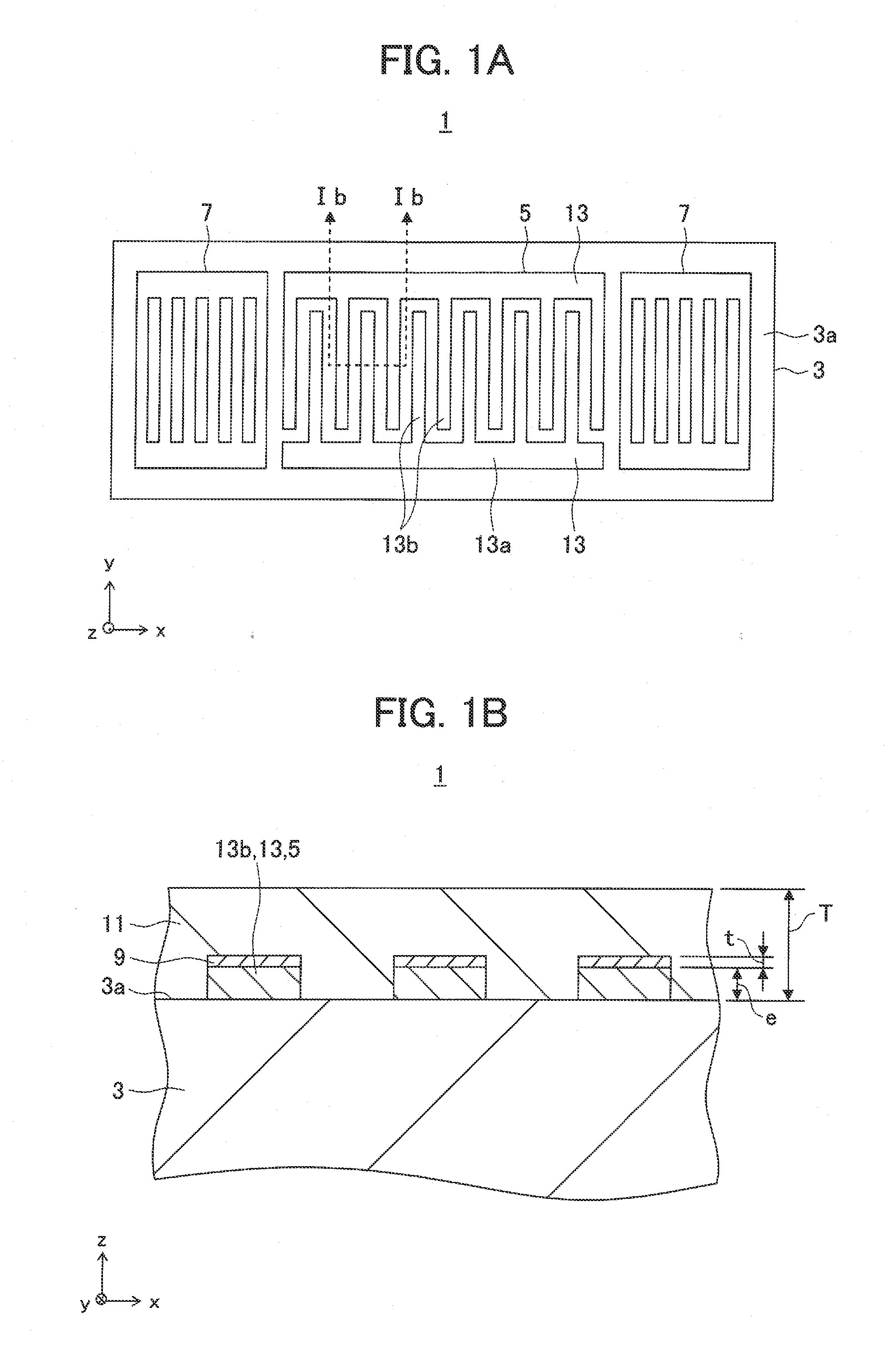
[0029]FIG. 1A is a plan view of a SAW element 1 according to a first embodiment of the present invention, and FIG. 1B is a cross-sectional view taken along a line Ib-Ib in FIG. 1A. Note that, in the SAW element 1, any direction may be upward or downward. However, in the following description, for convenience, a Cartesian coordinate system xyz is defined, the positive side of the z-direction (the front side from the surface of the paper in FIG. 1A and the upper side in the surface of the paper in FIG. 1B) is defined as the upper side, and the terms “upper surface”, “lower surface”, etc. are used based on this.
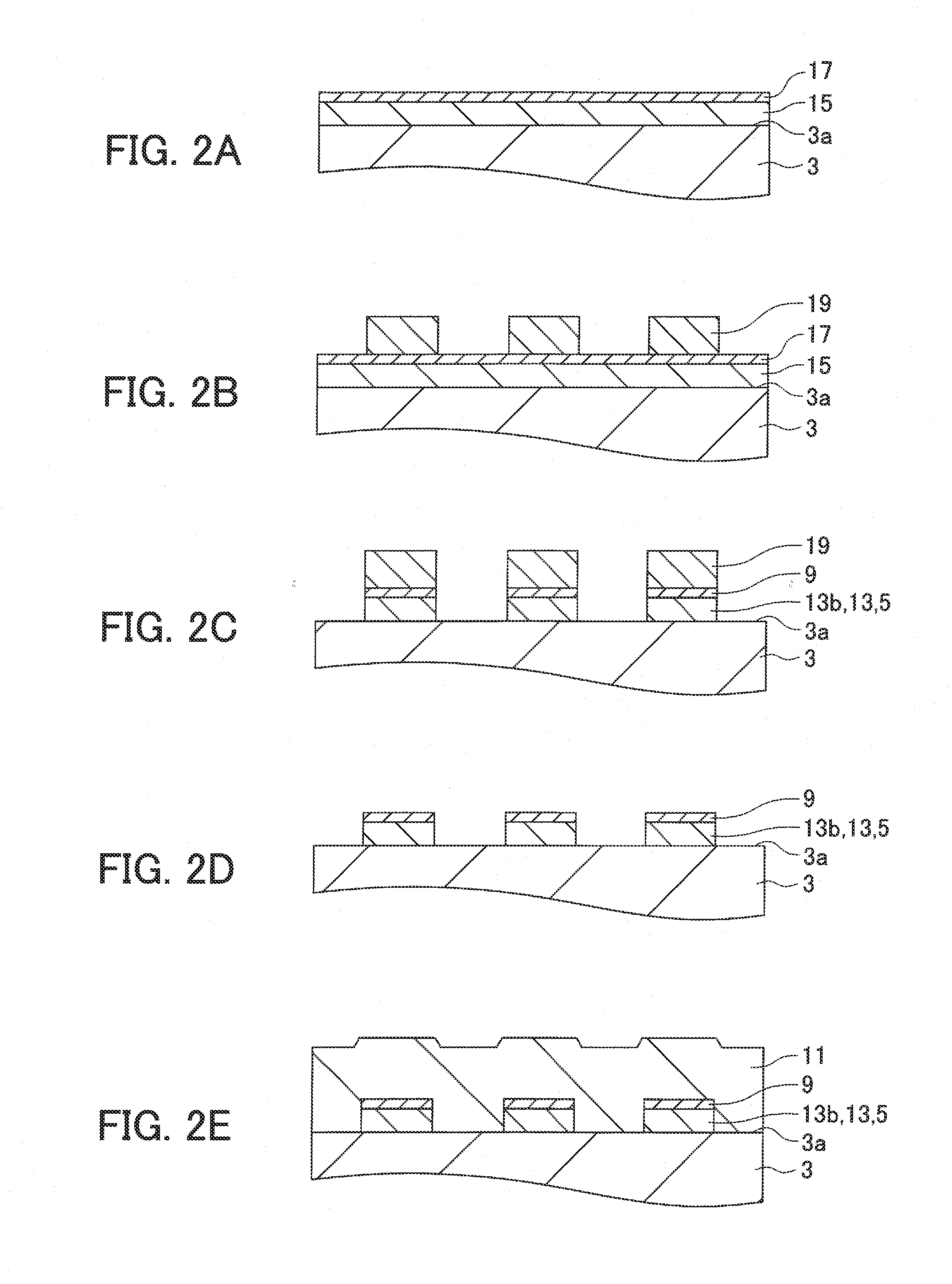
[0030]The SAW element 1 has a substrate 3, an IDT electrode 5 and reflectors 7 which are provided at an upper surface 3a of the substrate 3, a first film 9 (FIG. 1B) which is provided on the IDT electrode 5 and reflectors 7, and a protective layer 11 (FIG. 1B) which covers the upper surface 3a from the upper side of the firs...
second embodiment
[0123]FIG. 13A is a plan view which shows a SAW element 301 according to a second embodiment.
[0124]An IDT electrode 305 of the SAW element 301 is made of Al or an alloy which contains Al as a major component in the same way as the IDT electrode 5 in the first embodiment and has a pair of comb-shaped electrodes 313. Further, each comb-shaped electrode 313 has a bus bar 313a and a plurality of electrode fingers 313b in the same way as the comb-shaped electrodes 13 in the first embodiment.
[0125]Further, each comb-shaped electrode 313 has a plurality of dummy electrodes 313c extending between two or more electrode fingers 313b from the bus bar 313a toward the bus bar 313a side of the other comb-shaped electrode 313. Tip ends of the plurality of dummy electrodes 313c of each comb-shaped electrode 313 face the tips of the plurality of electrode fingers 313b of the other comb-shaped electrode 313 through tip gap portions G1. The width of a dummy electrode 313c (size in the x-direction) is ...
third embodiment
[0144]FIG. 16A is a plan view which shows a SAW element 401 according to a third embodiment.
[0145]The IDT electrode 5 of the SAW element 401 is the same as the IDT electrode 5 in the first embodiment. That is, the dummy electrodes 313c shown in the second embodiment are not provided. Further, the tips of the plurality of electrode fingers 13b of each comb-shaped electrode 13 face the bus bar 13a of the other comb-shaped electrode 13 through a plurality of tip gap portions G2. Note that, the IDT electrode 5 may be apodized in the same way as the second embodiment.
[0146]FIG. 16B is a perspective view in a region XVIb in FIG. 16A. Note that, the figure shows the state through the protective layer 11.
[0147]On the upper surface of the IDT electrode 5, the first film 9 is provided in the same way as the first embodiment. Further, in the SAW element 401, the second film 410 is arranged on the tip gap portions G2. The material of the second film 410 is the same as the material of the second...
PUM
 Abstract
Description
Claims
Application Information
 - R&D Engineer
- R&D Manager
- IP Professional
- Industry Leading Data Capabilities
- Powerful AI technology
- Patent DNA Extraction
Browse by: Latest US Patents, China's latest patents, Technical Efficacy Thesaurus, Application Domain, Technology Topic.
© 2024 PatSnap. All rights reserved.Legal|Privacy policy|Modern Slavery Act Transparency Statement|Sitemap