Power clamp for high voltage integrated circuits

a technology of power clamps and integrated circuits, which is applied in the direction of emergency protective circuit arrangements, emergency protective arrangements for limiting excess voltage/current, electrical equipment, etc., can solve the problems of gate oxide stress, drain/well voltage overstress, and difficult design of high voltage tolerant esd clamps using nominal devices

Active Publication Date: 2013-10-10
GLOBALFOUNDRIES SINGAPORE PTE LTD
View PDF6 Cites 17 Cited by
  • Summary
  • Abstract
  • Description
  • Claims
  • Application Information

AI Technical Summary

Problems solved by technology

Design of high voltage tolerant ESD clamps using nominal devices can be quite challenging.
During programming mode, the use of simple ESD clamps using nominal devices often present reliability issues such as gate oxide stress, drain/well voltage overstress, etc.
M...

Method used


Image

  • Power clamp for high voltage integrated circuits
  • Power clamp for high voltage integrated circuits
  • Power clamp for high voltage integrated circuits

Examples


Embodiment Construction

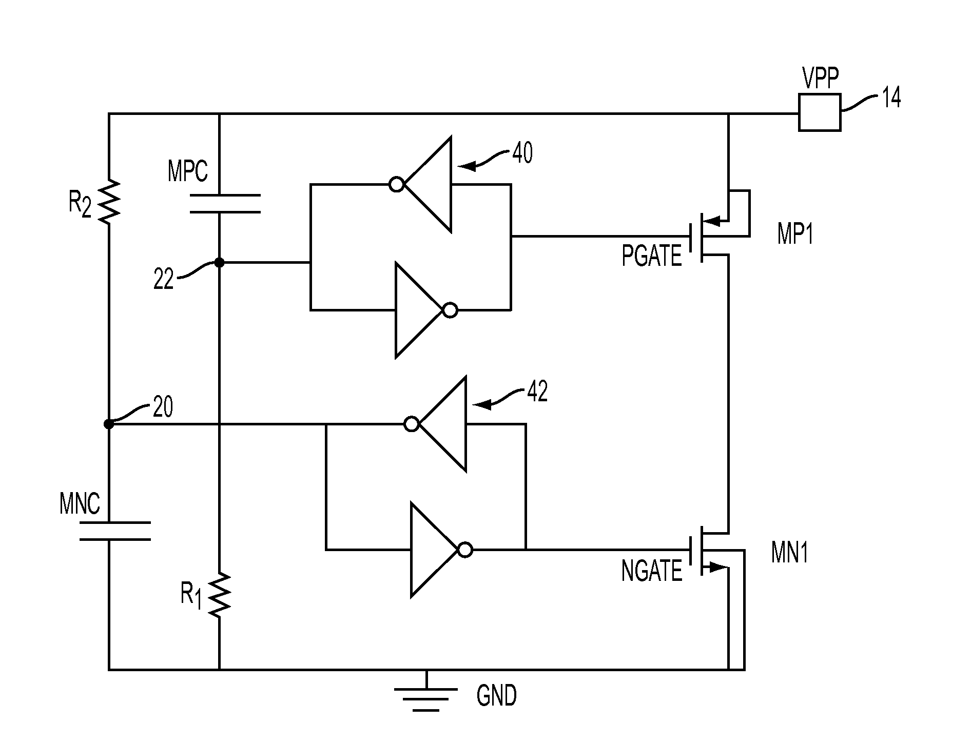
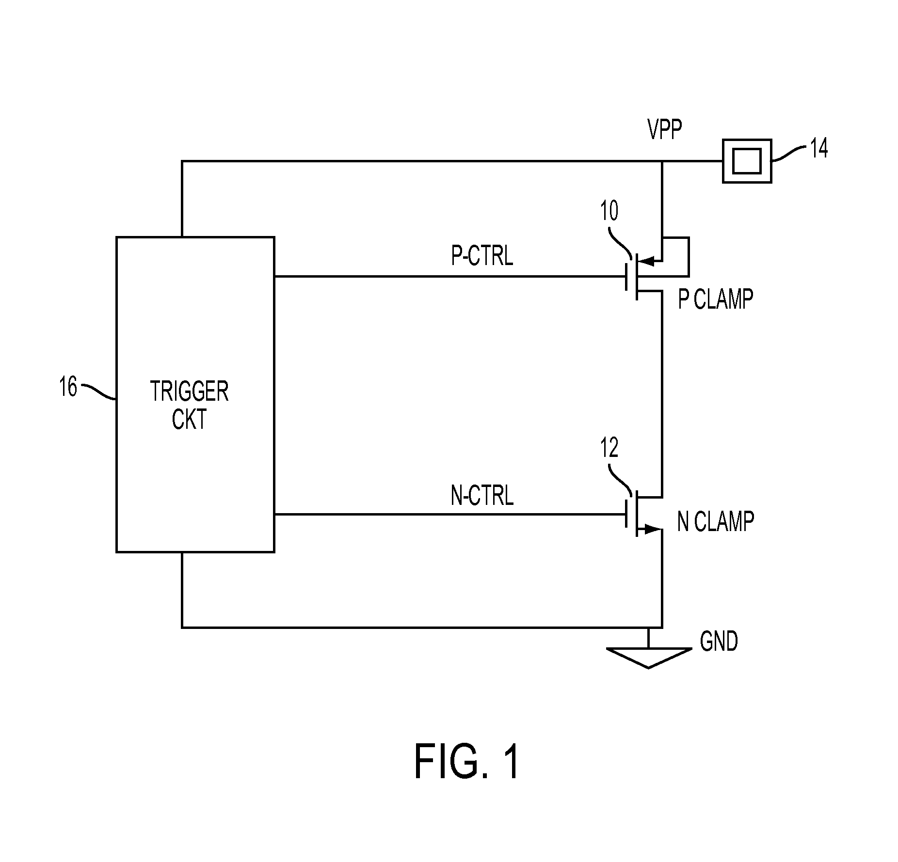
[0014]A PMOS / NMOS power clamp of the present disclosure is depicted in block diagram form in FIG. 1. P-Clamp 10 and N-Clamp 12 are ESD clamping devices connected in series between a voltage source pad 14 and ground. During normal pad operation, such as OTP memory programming, the gate of N-Clamp 12 is driven to a logic low and the gate of P-Clamp 10 is driven to a logic high. As both devices are driven off, there will be no oxide stress, no oxide / junction stress, and no leakage current. After an ESD event is detected by the trigger unit, clamping devices 10 and 12 will be driven on by clamping signals generated by trigger unit 16 to sink the current to ground. A logic low signal will be applied to P-Clamp 10 and a logic high signal will be applied to N-Clamp 12.

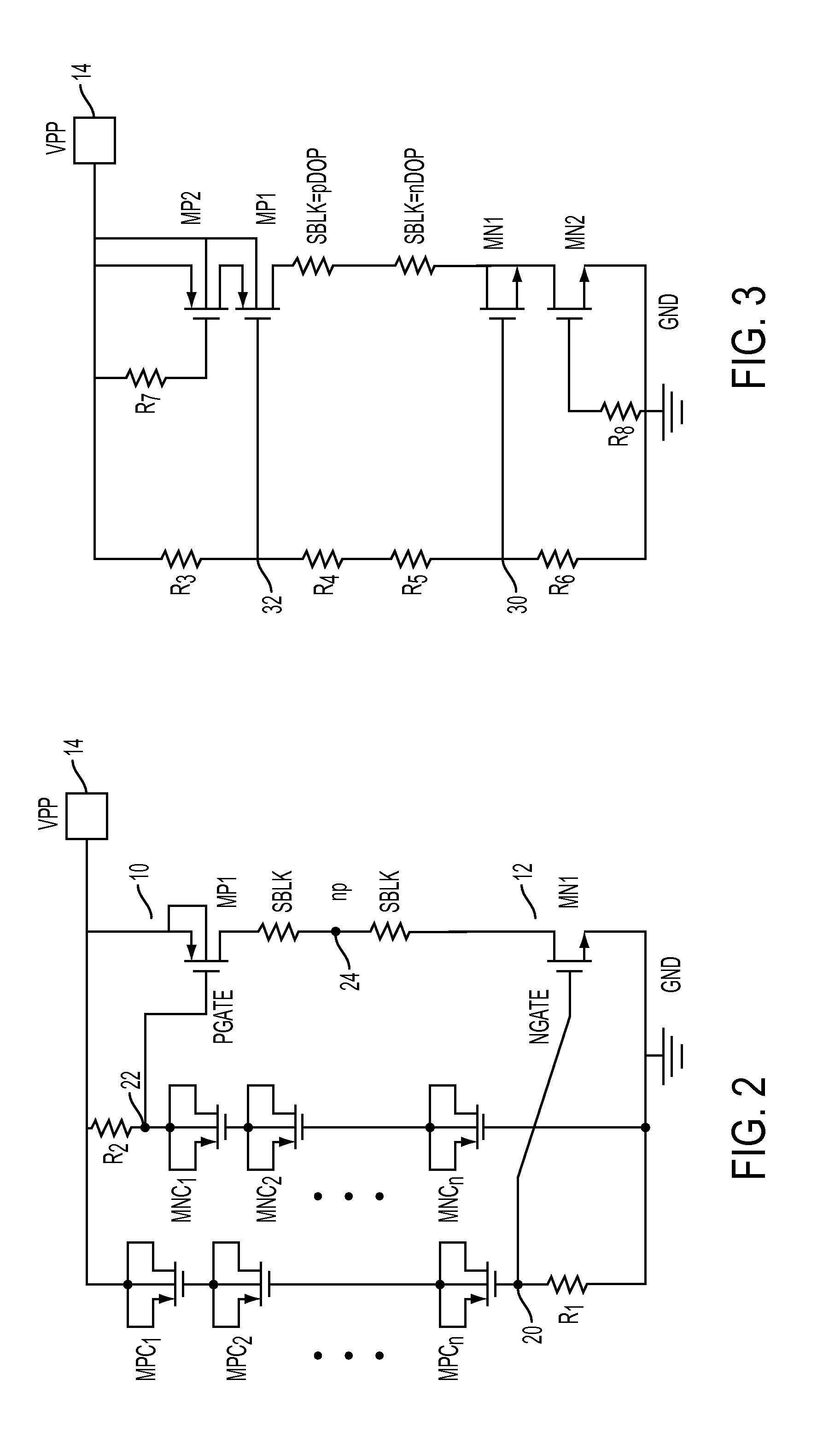
[0015]Buffering by the trigger unit is desirable to stabilize the clamping signals to avoid any mis-triggering of the clamping devices. One implementation for providing appropriate buffering is exemplified by the circuit diag...


PUM


Abstract

A clamp circuit includes both nmos and pmos devices connected in series between a voltage source terminal, such as an integrated circuit pad, and ground. A trigger unit, connected between the voltage source and ground, includes a plurality of output terminals coupled to the clamp circuit. The trigger unit is responsive to a voltage threshold, such as caused by an ESD occurrence, between the voltage source and ground to apply clamping signals at its output terminals to couple the voltage source terminal to ground through both nmos and pmos devices.

Description

BACKGROUND[0001]This disclosure relates to high voltage clamps for integrated circuits. The need for protection against electrostatic discharge (ESD) exists, for example, in applications including programming pads. Such applications may involve One Time Programmable (OTP) memories used in RFID, video game consoles, mobile phones, and the like.[0002]Design of high voltage tolerant ESD clamps using nominal devices can be quite challenging. During programming mode, the use of simple ESD clamps using nominal devices often present reliability issues such as gate oxide stress, drain / well voltage overstress, etc. A commonly used technique to overcome such problems is by stacking nmos FETs in a clamping device. An example of such technique is disclosed in U.S. Pat. No. 7,203,045. Multilevel stacking of nmos elements, however, reduces clamping efficiency with each added level. Reliability concerns exist with respect to drain junction voltages and gate oxide breakdown, as well as the possibil...

Claims


Application Information

Patent Timeline
IPC IPC(8): H02H9/04
CPCH02H9/046
Inventor PRABHU, MANJUNATHANATARAJAN, MAHADEVA IYERLAI, DA-WEIRYAN, SHAN
Owner GLOBALFOUNDRIES SINGAPORE PTE LTD
Why Eureka
Try Eureka