Optical antennas with enhanced fields and electron emission

a technology of optical antennas and electron emission, applied in the field of optical antennas with enhanced fields and electron emission, can solve the problems of high material cost, high material cost associated with the use of materials and manufacturing processes, and physical limitation of pv technology to less than 33% energy collection efficiency, etc., to achieve enhanced particular frequencies, improve the field intensity, and increase the packing density

Active Publication Date: 2013-11-07
PACIFIC INTEGRATED ENERGY
View PDF9 Cites 26 Cited by
  • Summary
  • Abstract
  • Description
  • Claims
  • Application Information

AI Technical Summary

Benefits of technology

[0013]In some embodiments, the electromagnetic (EM) fields of light are locally enhanced by physical features of a photon collector and conversion design. In an embodiment, using the electromagnetic wave nature of light, the electric and the magnetic fields of the light wave are enhanced using structural geometries and layering between conductor and insulator or dielectric layers. In another embodiment, metal-coated nanospherical particles create collective coupling of electrons to an incident electromagnetic wave. In some cases, the size of the particle and the metal determine the characteristics of this coupling, which is also called a plasmon wave. In another embodiment, plasmon waves create a strong local field enhancement.
[0038]In suitable instances, a ground plane, or anode collects the emitted electrons. The ground plane is connected to a load with appropriate matching conditions. In some embodiments, the load is advantageously a motor, a battery, a storage device or any other device that uses or collects the electrical energy generated by the energy collector disclosed herein or sense current intensity in the case of sensors or touchscreen applications. In one embodiment the anode has an inverted tapered structure pointing up towards the cathode, the cathode being the electron emitting tip of the conical structure. This creates a higher field disturbance between the cathode and anode, lowering the required field for emission.

Problems solved by technology

PV technology is limited physically to less than 33% energy collection efficiency by bandgap energy collection limitations and by semiconductor electrical resistance.
Additionally semiconductor-based PV has high costs associated with the materials used and the manufacturing process.
The material costs include the high cost to produce pure wafers and the use of rare and expensive materials.
The manufacturing costs include the huge capital cost to build a semiconductor facility, the control of toxic materials used and the cleanliness requirement to prevent any impurities from doping the product while under manufacture.
The large area requirement provides an inherent limitation to devices that use expensive processes because of the surface area cost to generate PV-based solar energy.
Therefore, there are cost restrictions for the use of inorganic PVs for many energy markets.
Another major downside for current PV technology is the use of toxic materials during processing of PV devices and in the final PV product.
After the end of life of current PV devices, the environmentally toxic or hazardous materials contained in such devices creates an environmental disposal problem.
Such devices have a net energy loss and amplify a signal using an external power source.
These devices consume more power than they produce and are not useful as energy collectors.
As promising as these new technologies are, most are restricted to collecting light using discrete quantum energy bands, which imposes the same inherent efficiency limitations as semiconductor PV technologies.
As with inorganic semiconductors, this approach has a downside because each new well or junction creates a layer that may interfere with (mask) the well or junction below it and increase the path length of both the light and the free charge, which increases the losses from absorption and electrical resistance.
Furthermore, nanotechnology and quantum dots still have issues with toxicity, with the ability to manufacture and with efficiency.

Method used


Image

  • Optical antennas with enhanced fields and electron emission
  • Optical antennas with enhanced fields and electron emission
  • Optical antennas with enhanced fields and electron emission

Examples


Embodiment Construction

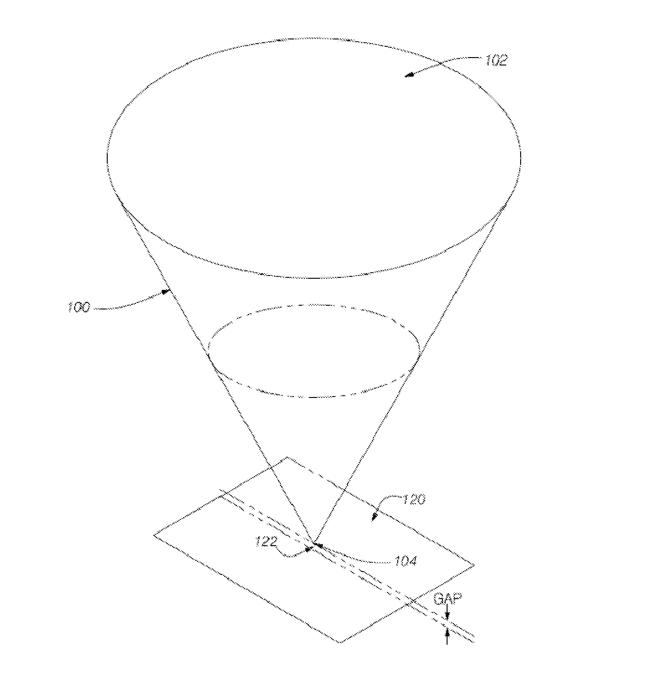
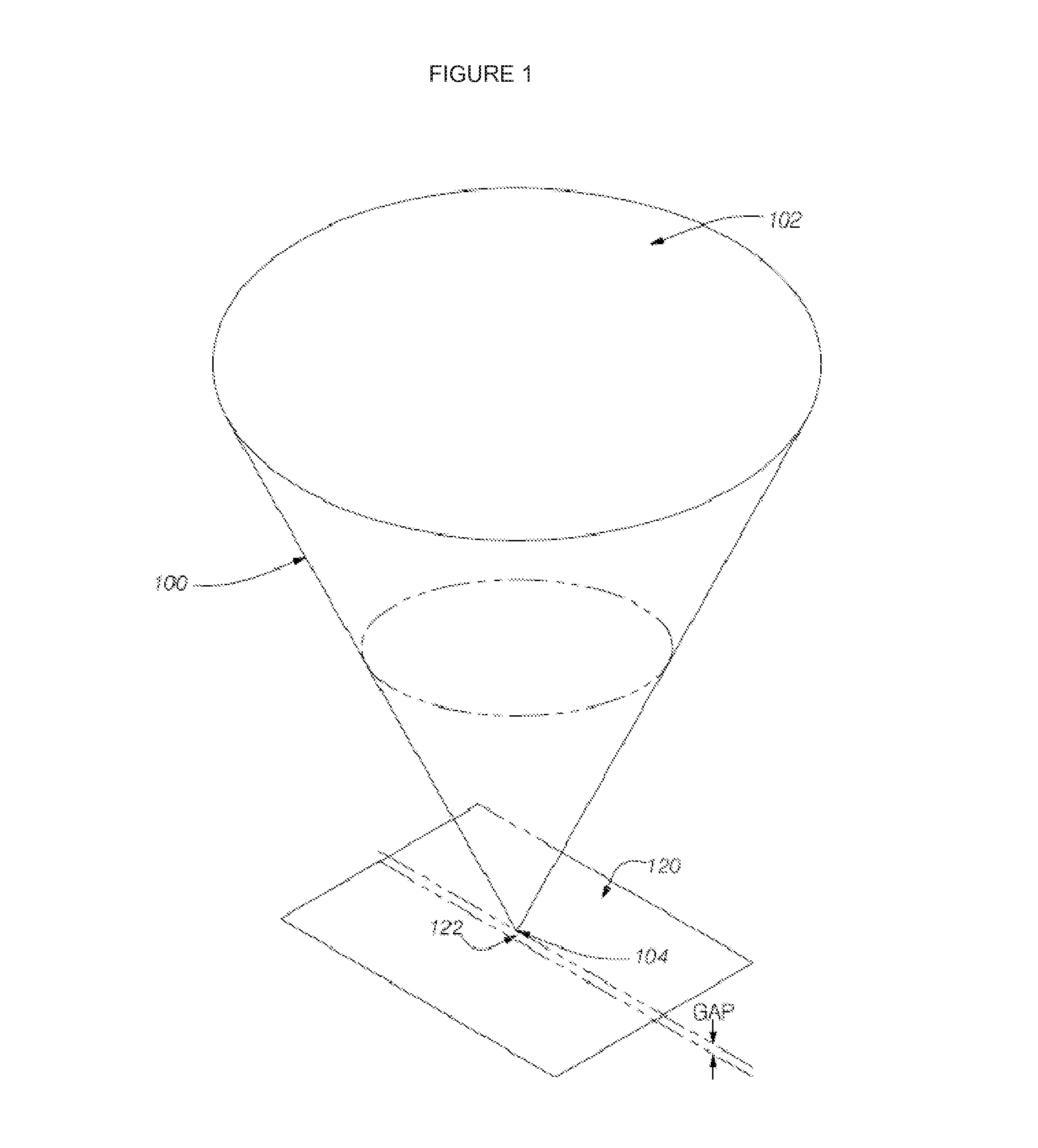
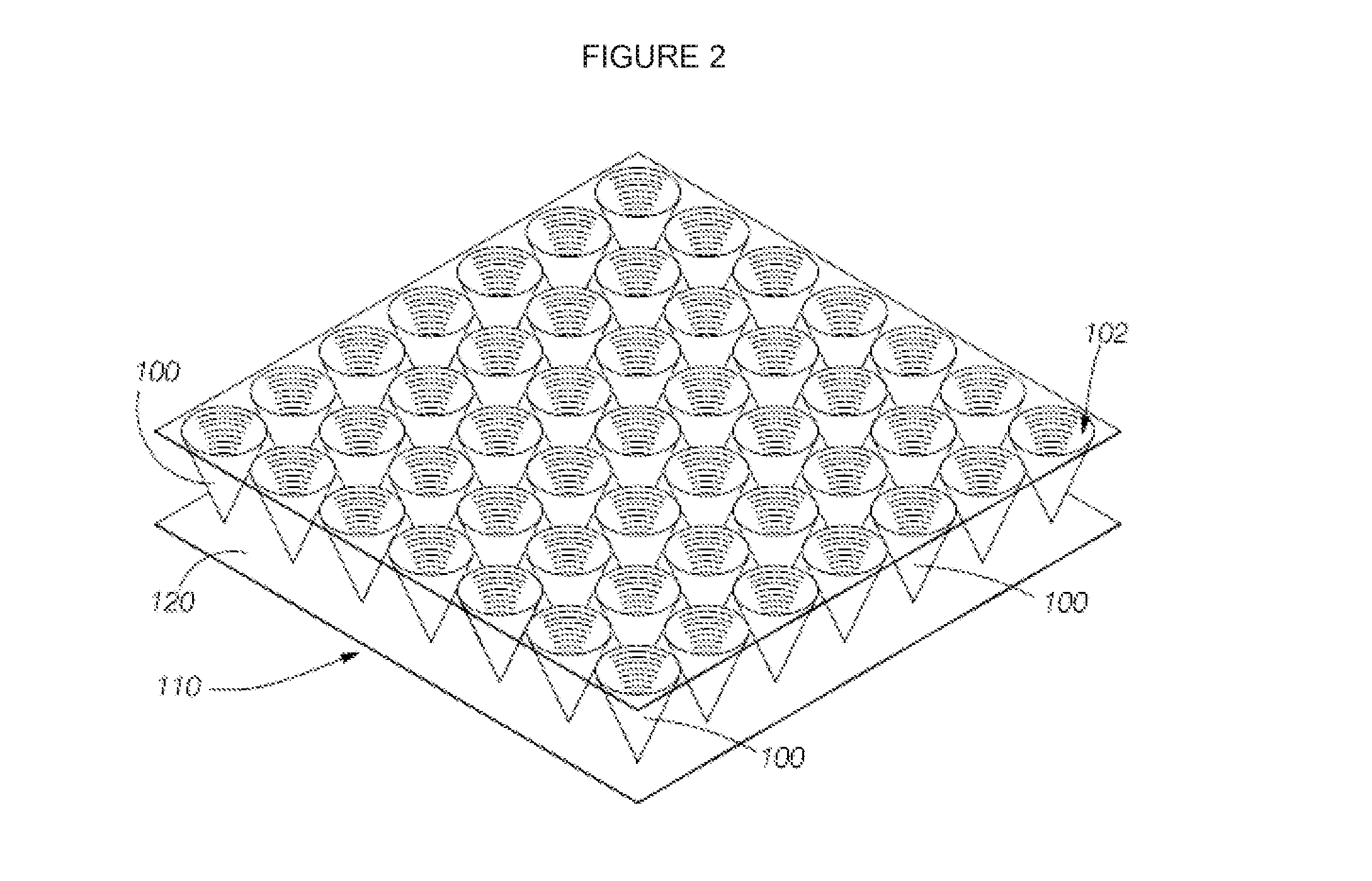
[0053]The drawings and the following description illustrate preferred embodiments of a system and method for implementing the present invention. In some embodiments, other shapes and configurations are also used to create the disclosed effect of collecting the electric field from the electromagnetic wave and funneling the electric field to a localized field region above a conducting plane where electrons are emitted from the distress field point or line.

[0054]The term “waveguide,” as used herein, refers to a structure or device that guides waves, such as electromagnetic energy.

[0055]The term “electromagnetic energy,” as used herein, refers to electromagnetic radiation (also “light” herein), which is a form of energy exhibiting wave-like behavior. Electromagnetic radiation includes radio waves, microwaves, infrared radiation, visible light, ultraviolet radiation, X-rays and gamma rays. Electromagnetic radiation includes photons, which is the quantum of the electromagnetic interaction...


PUM


Abstract

An electromagnetic energy collecting and sensing device is described. The device uses enhanced fields to emit electrons for energy collection. The device is configured to collect energy from visible light, infrared radiation and ultraviolet electromagnetic radiation. The device includes a waveguide with a geometry selected to enhance the electric field along a conductor to create a high, localized electric field, which causes electron emission across a gap to an electron return plane.

Description

CROSS-REFERENCE[0001]This application claims priority to U.S. Provisional Patent Application Ser. No. 61 / 352,697, filed on Jun. 8, 2010, which is entirely incorporated herein by reference.BACKGROUND OF THE INVENTION[0002]Traditionally, ultraviolet (UV), visible and infrared electromagnetic or light energy is collected using semiconductors with bandgap energies tuned to the desired photon energy to be collected. Alternatively, light energy may be converted into thermal energy by an absorber and then the heat energy may be collected by traditional thermal energy collectors, such as sterling engines, steam engines or other methods. These major solar energy collection technologies may be further grouped as follows: 1) inorganic, semiconductor based photovoltaic (“PV”) generation, 2) organic based PV generation, 3) nanotechnology, which includes carbon nanotubes and quantum dots, and 4) solar thermal or solar concentrator technologies. Silicon (semiconductor-based) PV technologies, solar...

Claims


Application Information

Patent Timeline
Patent Type & Authority Applications(United States)
IPC IPC(8): G02B6/00
CPCG02B6/00B82Y20/00G02B6/1226H01L31/035209H01Q21/064H01L31/0547Y02E10/52H01L31/052
Inventor LAYTON, PHILLIP J.KRUGLICK, EZEKIELACHOUR, MAHA
Owner PACIFIC INTEGRATED ENERGY
Why Eureka
Try Eureka