CMOS pixel control method

a pixel control and pixel technology, applied in the field of image sensors, can solve the problems of unwanted noise in the image, adversely affecting the measurement, etc., and achieve the effect of facilitating addressing

Inactive Publication Date: 2014-01-02
STMICROELECTRONICS (GRENOBLE 2) SAS
View PDF8 Cites 4 Cited by
  • Summary
  • Abstract
  • Description
  • Claims
  • Application Information

AI Technical Summary

Benefits of technology

[0006]An embodiment provides a method for controlling a CMOS pixel, which facilitates addressing at least some of the disadvantages of existing control methods.
[0007]An embodiment provides a multiple integration period control method, which facilitates introducing less unwanted noise into the images than existing methods.

Problems solved by technology

For high light intensities, the photocurrent may be such that the discharge of the junction capacitance during the integration phase adversely affects the measurement.
Such methods enable to extend the dynamic range of the sensor, but however have the disadvantage of introducing unwanted noise into the images.

Method used


Image

  • CMOS pixel control method
  • CMOS pixel control method
  • CMOS pixel control method

Examples


Embodiment Construction

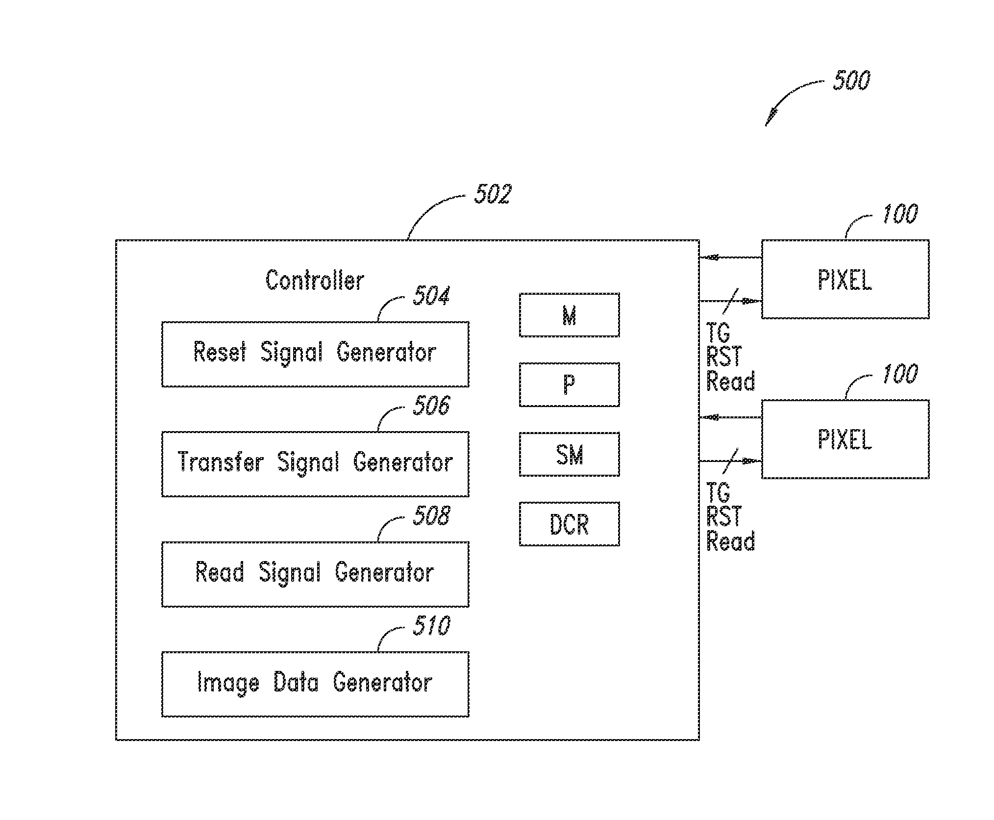
[0030]In the following description, numerous specific details are given to provide a thorough understanding of embodiments. The embodiments can be practiced without one or more of the specific details, or with other methods, components, materials, etc. In other instances, well-known structures, materials, or operations, such as, for example, transistors, photodiodes, processors, controllers, power supplies, etc., are not shown or described in detail to avoid obscuring aspects of the embodiments.

[0031]Reference throughout this specification to “one embodiment” or “an embodiment” means that a particular feature, structure, or characteristic described in connection with the embodiment is included in at least one embodiment. Thus, the appearances of the phrases “in one embodiment”“according to an embodiment” or “in an embodiment” and similar phrases in various places throughout this specification are not necessarily all referring to the same embodiment. Furthermore, the particular featu...


PUM


Abstract

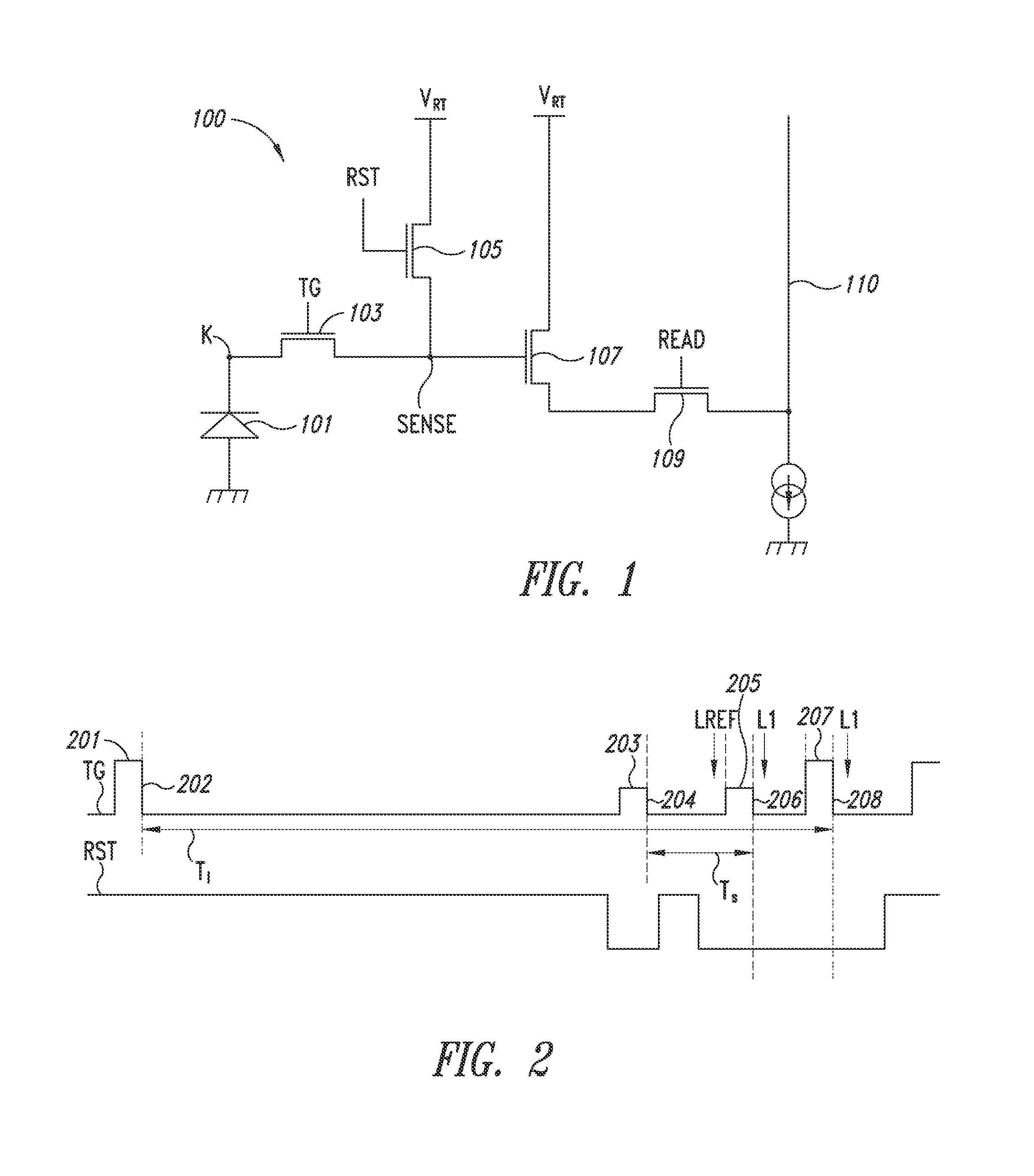
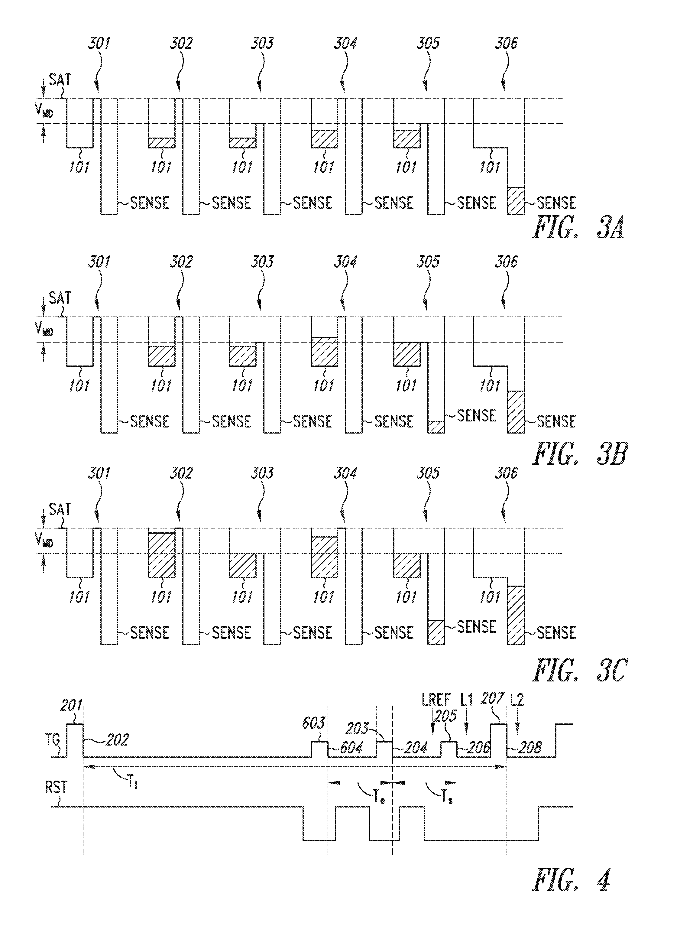
A method for controlling a pixel including at least one photodiode capable of being connected to a sense node, the method including the steps of: a) at the beginning and at the end of a first integration period included within a second integration period, controlling the pixel to transfer the charges stored in the photodiode above a first threshold onto the sense node; and b) at an intermediate time between the beginning of the second period and the beginning of the first period, controlling the pixel to transfer the charges stored in the photodiode above the first threshold onto the sense node.

Description

BACKGROUND[0001]1. Technical Field[0002]The present disclosure relates to image sensors, including CMOS sensors with a multiple integration period, called high-dynamics sensors, and to methods of controlling pixels of such sensors.[0003]2. Description of the Related Art[0004]A CMOS image sensor pixel essentially comprises a photodiode used in reverse mode, having its junction capacitance discharged by a photocurrent according to a received light intensity. The measurement of the illumination level received by a pixel is performed by measurement of the voltage across the photodiode at selected times, among which the end of a so-called image acquisition or integration period, before and after which the pixel is reset by recharging of its photodiode. The decrease of the voltage across the photodiode during the integration is proportional to the received light intensity. For high light intensities, the photocurrent may be such that the discharge of the junction capacitance during the in...

Claims


Application Information

Patent Timeline
Patent Type & Authority Applications(United States)
IPC IPC(8): H04N5/335
CPCH04N5/335H04N25/575H04N25/58H04N25/583H04N25/589H04N25/623H04N25/00H04N25/57H04N25/62H04N3/155
Inventor DESCHAMPS, BENOIT
Owner STMICROELECTRONICS (GRENOBLE 2) SAS
Why Eureka
Try Eureka