Pulse output circuit, display device, and electronic device

a technology of output circuit and output circuit, which is applied in the field of pulse output circuit, can solve the problems of easy deterioration of transistors, variation in electrical characteristics of transistors, and deterioration of transistors, so as to reduce transistor stress, suppress transistor deterioration, and suppress transistor variation in electrical characteristics

Active Publication Date: 2014-01-23
SEMICON ENERGY LAB CO LTD
View PDF6 Cites 34 Cited by
  • Summary
  • Abstract
  • Description
  • Claims
  • Application Information

AI Technical Summary

Benefits of technology

[0009]For example, in the shift register in Patent Document 1, when a pulse signal output from a pulse output circuit is at low level, the potential of a gate of a transistor that controls whether to set the output pulse signal to high level (e.g., the transistor 105 in FIG. 1B in Patent Document 1) is held at a potential VSS for a certain period. At this time, the potential of a source or a drain of the above transistor changes repeatedly in accordance with a clock signal; thus, the transistor is subjected to stress. This causes deterioration of the transistor. In particular, the time during which the transistor is subjected to the stress is extremely long in the shift register in Patent Document 1; thus, the transistor easily deteriorates and the electrical characteristics keeps varying.
[0011]In consideration of the above problems, an object of one embodiment of the present invention is to suppress the stress applied to a transistor that controls whether to set the output pulse signal to high level as well as suppressing generation of defective operation.
[0012]In one embodiment of the present invention, in a period during which a pulse signal output from a pulse output circuit is at low level, the potential of a gate of a transistor that controls whether to set the pulse signal to high level is not set to a constant value but intermittently set to a value higher than the potential VSS. Accordingly, the stress to the transistor can be suppressed.
[0014]With one embodiment of the present invention, without lengthening the channel length of a transistor that controls whether to set the output pulse signal to high level, the stress to the transistor can be reduced. As a result, deterioration of the transistor can be suppressed, and variation in electrical characteristics can be suppressed.

Problems solved by technology

However, conventional pulse output circuits have a problem of variation in electrical characteristics of a transistor when the transistor deteriorates owing to high amplitude of a clock signal.
This causes deterioration of the transistor.
In particular, the time during which the transistor is subjected to the stress is extremely long in the shift register in Patent Document 1; thus, the transistor easily deteriorates and the electrical characteristics keeps varying.
However, if the channel length of the transistor that controls whether to set the output pulse signal to high level is lengthened, a problem of increasing the possibility of causing defective operation due to the delay of the output pulse signal by parasitic capacitance or the like arises, for example.

Method used


Image

  • Pulse output circuit, display device, and electronic device
  • Pulse output circuit, display device, and electronic device
  • Pulse output circuit, display device, and electronic device

Examples


embodiment 1

[0032]In this embodiment, an example of a pulse output circuit will be described.

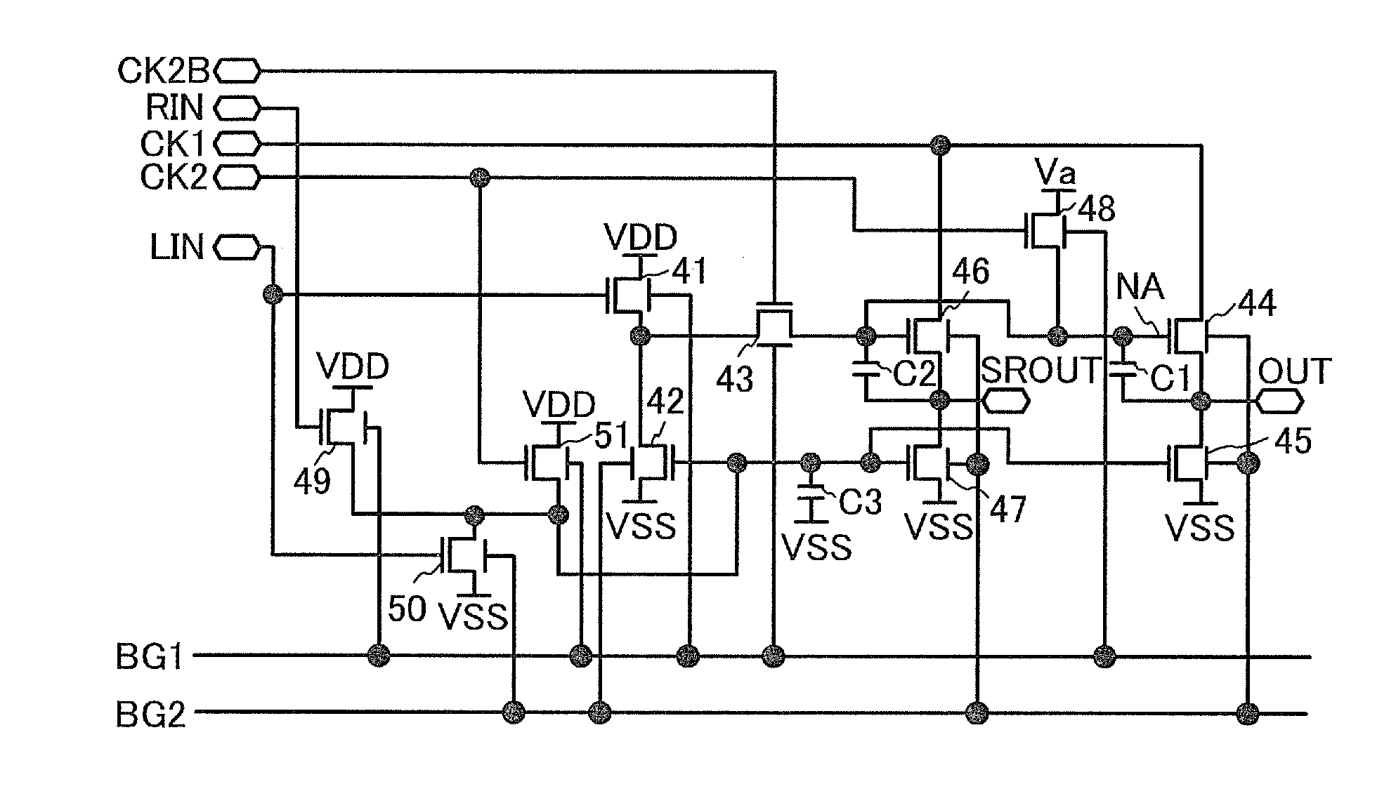
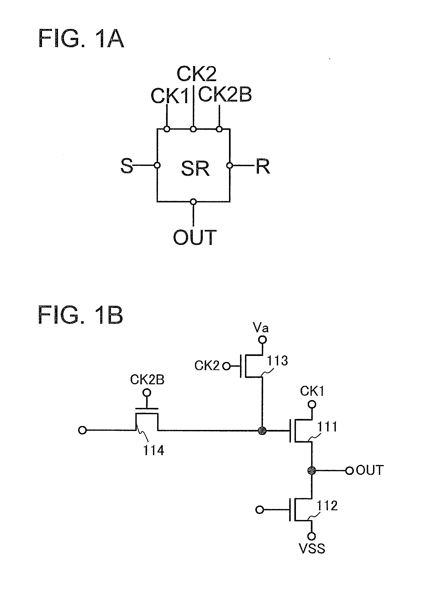
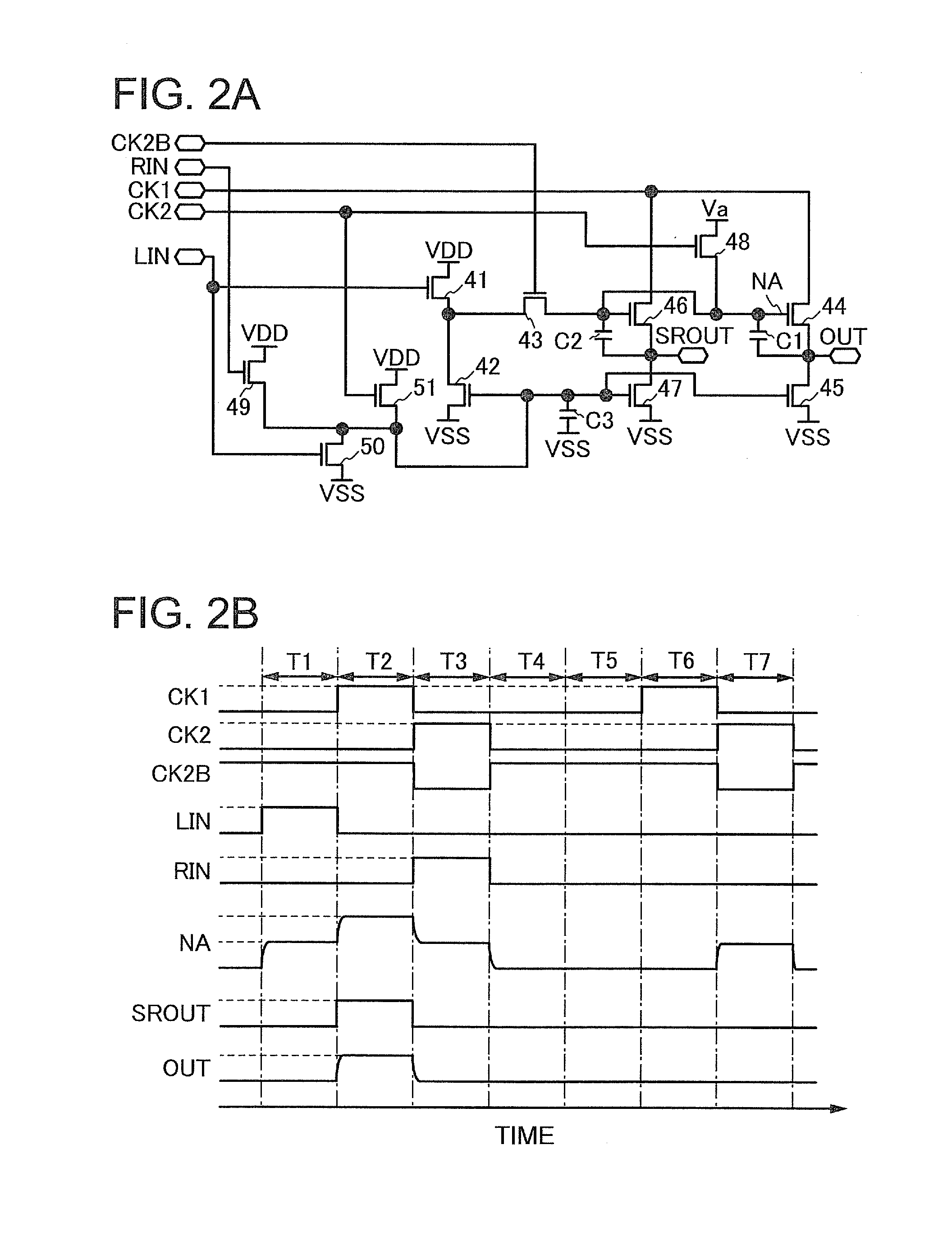
[0033]FIGS. 1A and 1B illustrate an example of a pulse output circuit of this embodiment. As illustrated in FIG. 1A, a pulse output circuit SR has a function of generating a pulse signal as an output signal OUT in accordance with input signals such as a set signal S, a reset signal R, a clock signal CK1, a clock signal CK2, and a clock signal CK2B. The clock signal CK2B can be an inverted signal of the clock signal CK2 or another clock signal.

[0034]The pulse output circuit SR illustrated in FIG. 1A includes transistors 111 to 114 as illustrated in FIG. 1B. The transistors 111 to 114 have the same conductivity type. The conduction of each of the transistors 111 to 114 is controlled by one or some of the set signal S, the reset signal R, the clock signal CK1, the clock signal CK2, and the clock signal CK2B. Note that an element other than the transistors 111 to 114 may be provided in the pulse output circ...

embodiment 2

[0124]In this embodiment, examples of a display device including the pulse output circuit of Embodiment 1 is described with reference to FIGS. 7A, 7B1, and 7B2, FIG. 8, FIG. 9, and FIGS. 10A and 10B.

[0125]The display device in FIG. 7A includes a pixel portion 201 and a driver circuit portion 202.

[0126]The pixel portion 201 includes a plurality of pixel circuits 211 arranged in X rows (X is a natural number of greater than or equal to 2) and Y columns (Y is a natural number of greater than or equal to 2). The driver circuit portion 202 includes driver circuits such as a gate driver 221 and a source driver 223.

[0127]The gate driver 221 includes a shift register including a plurality of stages of pulse output circuits described in Embodiment 1 (e.g., the shift register 30 illustrated in FIG. 5A). For example, the gate driver 221 has a function of controlling potentials of scan lines GL_1 to GL_X in accordance with a pulse signal output from the shift register. Note that a plurality of ...

embodiment 3

[0224]In this embodiment, examples of an electronic device provided with a panel using the display device of Embodiment 2 are described with reference to FIGS. 11A to 11D.

[0225]The electronic device in FIG. 11A is an example of a portable information terminal.

[0226]The electronic device illustrated in FIG. 11A includes a housing 1011, a panel 1012 provided in the housing 1011, a button 1013, and a speaker 1014.

[0227]The housing 1011 may be provided with a connection terminal for connecting the electronic device to an external device and a button for operating the electronic device.

[0228]The panel 1012 may be formed using the display device in Embodiment 2.

[0229]The panel 1012 may be a touch panel; in this case, touch detection can be performed on the panel 1012. As the touch panel, an optical touch panel, a capacitive touch panel, a resistive touch panel, or the like can be used, for example.

[0230]The button 1013 is provided on the housing 1011. For example, when the button 1013 is ...


PUM


Abstract

An object is to suppress the stress applied to a transistor as well as suppressing generation of defective operation. In a pulse output circuit having a function of outputting a pulse signal and including a transistor that controls whether to set the pulse signal to high level, in a period during which the pulse signal output from the pulse output circuit is at low level, the potential of a gate of a transistor is not set to a constant value but intermittently set to a value higher than the potential VSS. Accordingly, the stress to the transistor can be suppressed.

Description

BACKGROUND OF THE INVENTION[0001]1. Field of the Invention[0002]The present invention relates to a pulse output circuit. Further, the present invention relates to a display device. Furthermore, the present invention relates to an electronic device.[0003]2. Description of the Related Art[0004]In recent years, for the purpose of simplifying the manufacturing process, circuits composed of only transistors having the same conductivity type (also referred to as circuits composed of only n-channel transistors or p-channel transistors) have been developed.[0005]As an example of the circuits composed of only transistors having the same conductivity type, a pulse output circuit included in a shift register can be given.[0006]For example, Patent Document 1 discloses a shift register including a plurality of stages of pulse output circuits that use pulses of a clock signal to generate pulses of a pulse signal. Further, Patent Document 1 discloses a shift register that utilizes bootstrap to pre...

Claims


Application Information

Patent Timeline
Patent Type & Authority Applications(United States)
IPC IPC(8): G11C19/18
CPCG11C19/188G11C19/184G11C19/28G09G3/3688G09G3/3648G09G2310/0286
Inventor MIYAKE, HIROYUKI
Owner SEMICON ENERGY LAB CO LTD
Why Eureka
Try Eureka