
Heterogeneous integration of microfluidic devices in package structures

a technology of microfluidic devices and package structures, applied in the direction of solid-state devices, diaphragms, printed circuit assembling, etc., can solve the problems of fluid pumping in microfluidic devices, and achieve the effect of avoiding fluid pumping

Active Publication Date: 2014-03-27
INTEL CORP
View PDF3 Cites 30 Cited by
  • Summary
  • Abstract
  • Description
  • Claims
  • Application Information

AI Technical Summary

Benefits of technology

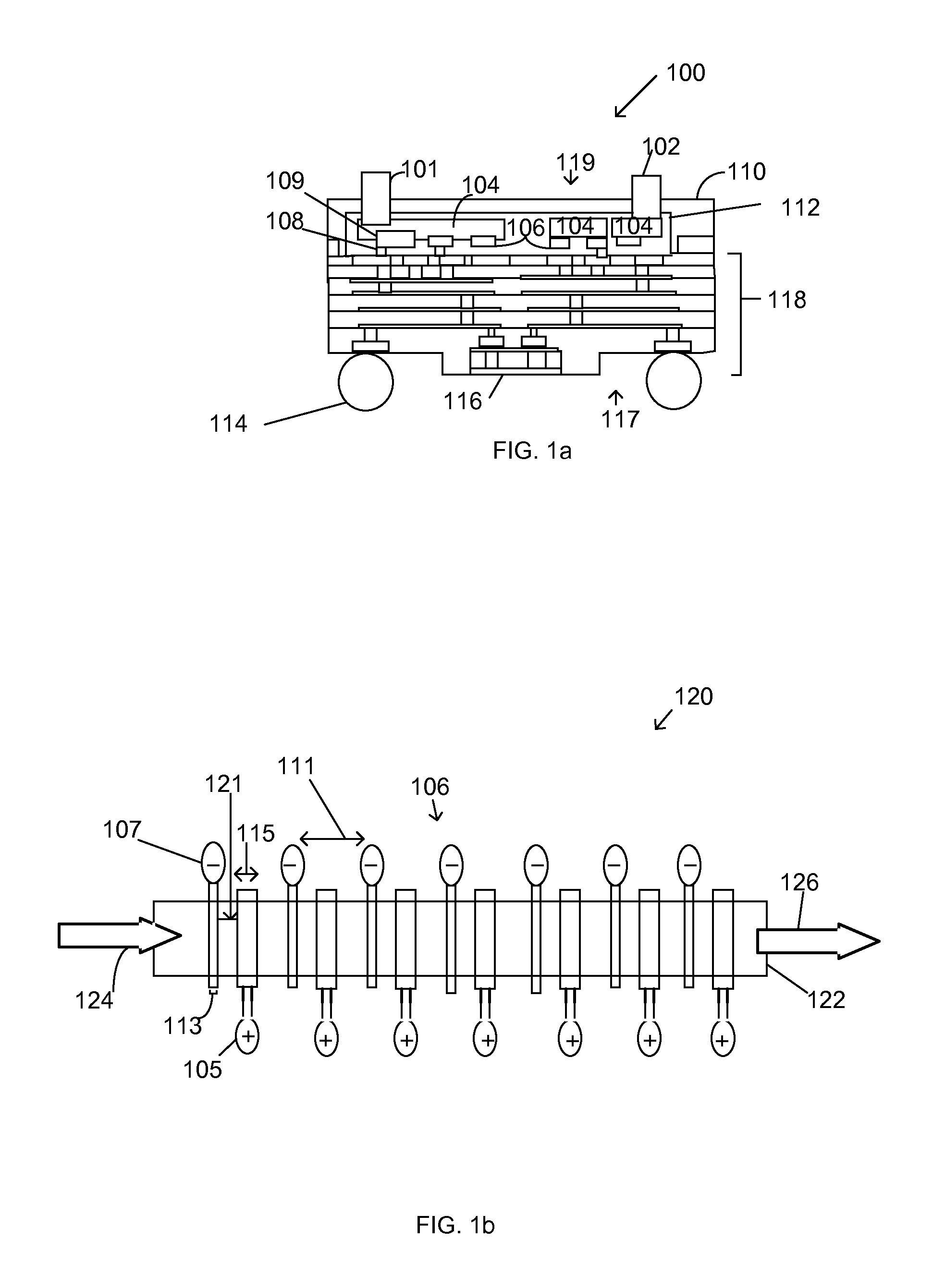
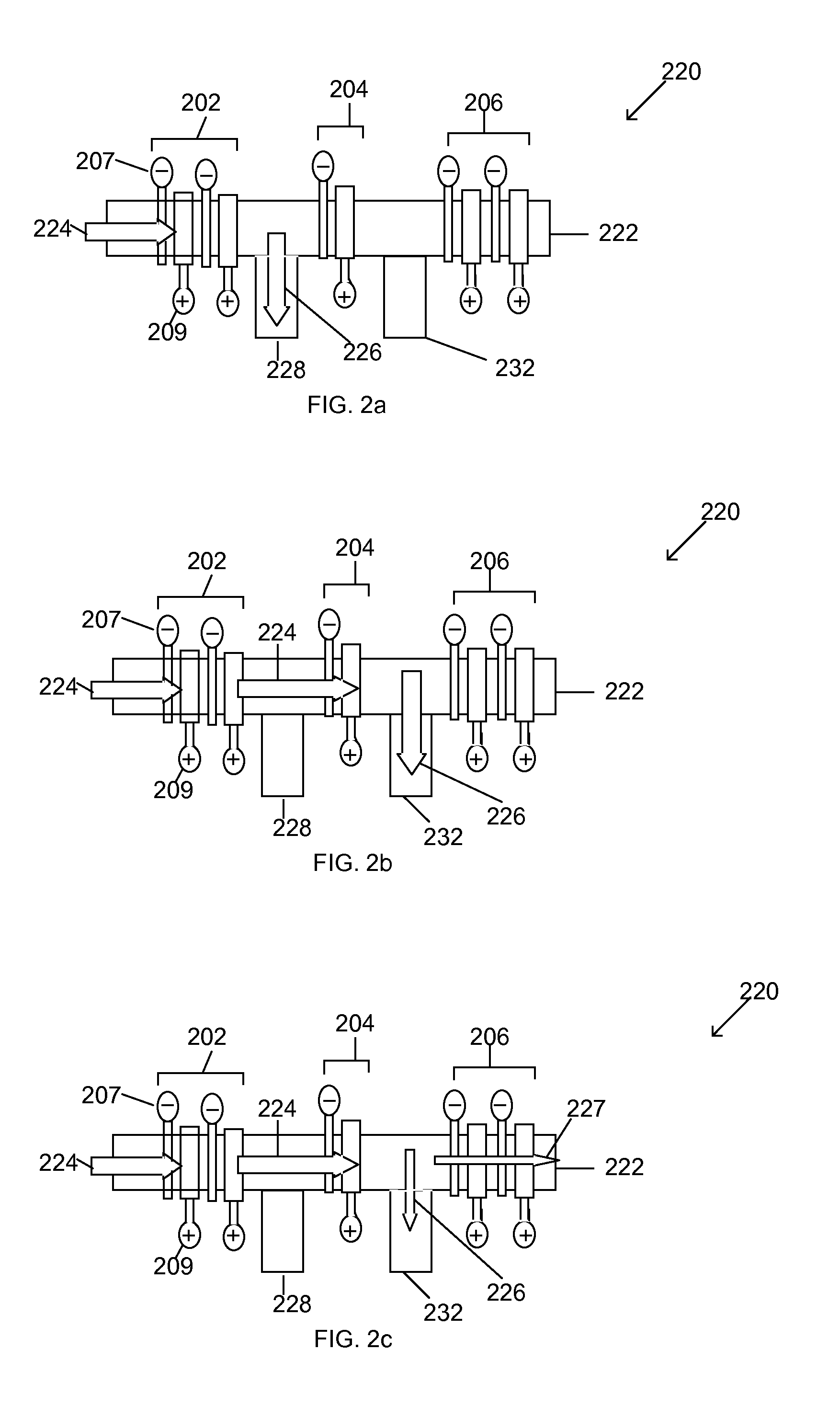
The patent describes a method of integrating microfluidic devices with other components, such as a package structure, using asymmetric electrodes to control the movement of fluids in the microfluidic device. This allows for precise control of fluid movement and the creation of a low-cost, small-form factor integration of microfluidic systems-on-package structures. The technical effects of this invention include improved control of fluid movement, reduced parabolic velocity profile, and improved pumping of fluids in microfluidic devices.

Problems solved by technology

Currently, pumping of fluid in microfluidics devices can be challenging, since pressure driven flows can have a parabolic velocity profile over a given cross-section of the microfluidic device, such as when the fluid flows through a fluid channel region within the microfluidic device.

Method used


Image

  • Heterogeneous integration of microfluidic devices in package structures
  • Heterogeneous integration of microfluidic devices in package structures
  • Heterogeneous integration of microfluidic devices in package structures

Examples


Embodiment Construction

[0011]In the following detailed description, reference is made to the accompanying drawings that show, by way of illustration, specific embodiments in which the methods and structures may be practiced. These embodiments are described in sufficient detail to enable those skilled in the art to practice the embodiments. It is to be understood that the various embodiments, although different, are not necessarily mutually exclusive. For example, a particular feature, structure, or characteristic described herein, in connection with one embodiment, may be implemented within other embodiments without departing from the spirit and scope of the embodiments. In addition, it is to be understood that the location or arrangement of individual elements within each disclosed embodiment may be modified without departing from the spirit and scope of the embodiments. The following detailed description is, therefore, not to be taken in a limiting sense, and the scope of the embodiments is defined only...


PUM

PropertyMeasurementUnit
Volumeaaaaaaaaaa
Volumeaaaaaaaaaa
Widthaaaaaaaaaa

Abstract

Methods of forming a microelectronic packaging structure and associated structures formed thereby are described. Those methods may include attaching a microfluidic die to a package structure, wherein the microfluidic die comprises a plurality of asymmetric electrodes that may be coupled with signal pads disposed within the package structure.

Description

BACK GROUND OF THE INVENTION[0001]Microelectromechanical systems (MEMS) devices are micro or nano devices that integrate mechanical and electrical elements on a common substrate, typically using microfabrication technology. MEMS devices can include actuators, sensors, switches, accelerometers, modulators, optical devices and microfluidic devices. Microfluidic devices can operate to control the flow of fluids across portions of the microfluidic device.[0002]Currently, pumping of fluid in microfluidics devices can be challenging, since pressure driven flows can have a parabolic velocity profile over a given cross-section of the microfluidic device, such as when the fluid flows through a fluid channel region within the microfluidic device. This parabolic velocity may result in a near zero velocity of the fluid flow at the walls of the channel, and a maximum velocity of the fluid flow at the center of the channel, for example.BRIEF DESCRIPTION OF THE DRAWINGS[0003]While the specificatio...

Claims


Application Information

Patent Timeline
IPC IPC(8): B01D43/00H05K3/30
CPCH05K1/0212H05K1/185H05K3/0097H05K2201/097H05K2203/1536H05K2203/308H01L2924/1815H01L2224/04105H01L2224/12105H01L2924/18162H01L21/568Y10T29/4913H05K1/0272H01L24/19H01L24/20H01L25/50H01L2224/18
Inventor TEH, WENG HONGLIN, KEVINEID, FERASMA, QING
Owner INTEL CORP
Learn More