Fabricating method of non-volatile memory structure

Active Publication Date: 2014-07-31
MACRONIX INT CO LTD
1 Cites 0 Cited by

AI-Extracted Technical Summary

Problems solved by technology

However, if the tunnel oxide layer under the polysilicon floating gate has defects, it can easily cause a leakage current in the device and affect the reliability of the device.
However, a flash memory may suffer from a second bit effect.
In addition, the length of the channel is reduced as...

Method used

[0043]Thereafter, a second conductive type doped region 120 is formed in the substrate 100 between the adjacent charge storage structures 116. The second conductive type doped region 120 has an overlap region R with each of the charge storage structures 116. In addition, the second conductive type doped region 120 divides the first conductive type doped layer 102 into a plurality of first conductive type doped regions 102a that are separated from each other. The overlap region R of the second conductive type doped region 120 and each of the charge storage structures 116 needs to be sufficient for the charge storage structure 116 located in the overlap region R to function as an effective charge storage region. Moreover, on condition that a program verify condition is met, the size of the overlap region R may be decreased to reduce the second bit effect and program disturbance that are generated during operation. A ratio of a width W1 of the overlap region R of the second c...

Benefits of technology

[0008]An embodiment of the invention provides a non-volatile memory structure for redu...

Abstract

A fabricating method for fabricating a non-volatile memory structure including the following steps is provided. A first conductive type doped layer is formed in a substrate. A plurality of stacked structures is formed on the substrate, and each of the stacked structures includes a charge storage structure. A first dielectric layer is formed on the substrate between the adjacent stacked structures. A second conductive type doped region is formed in the substrate between the adjacent charge storage structures. The second conductive type doped region has an overlap region with each of the charge storage structures. In addition, the second conductive type doped region divides the first conductive type doped layer into a plurality of first conductive type doped regions that are separated from each other. A conductive layer is formed on the first dielectric layer.

Application Domain

Semiconductor/solid-state device manufacturingSemiconductor devices

Technology Topic

EngineeringStorage structure +2

Image

  • Fabricating method of non-volatile memory structure
  • Fabricating method of non-volatile memory structure
  • Fabricating method of non-volatile memory structure

Examples

  • Experimental program(1)

Example

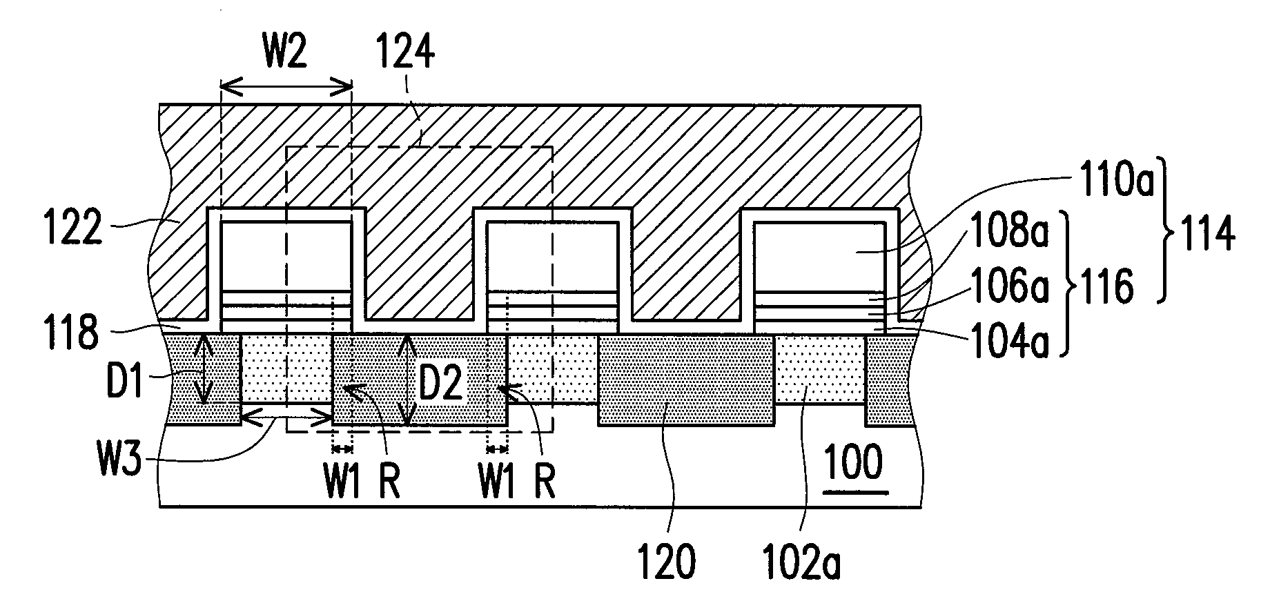
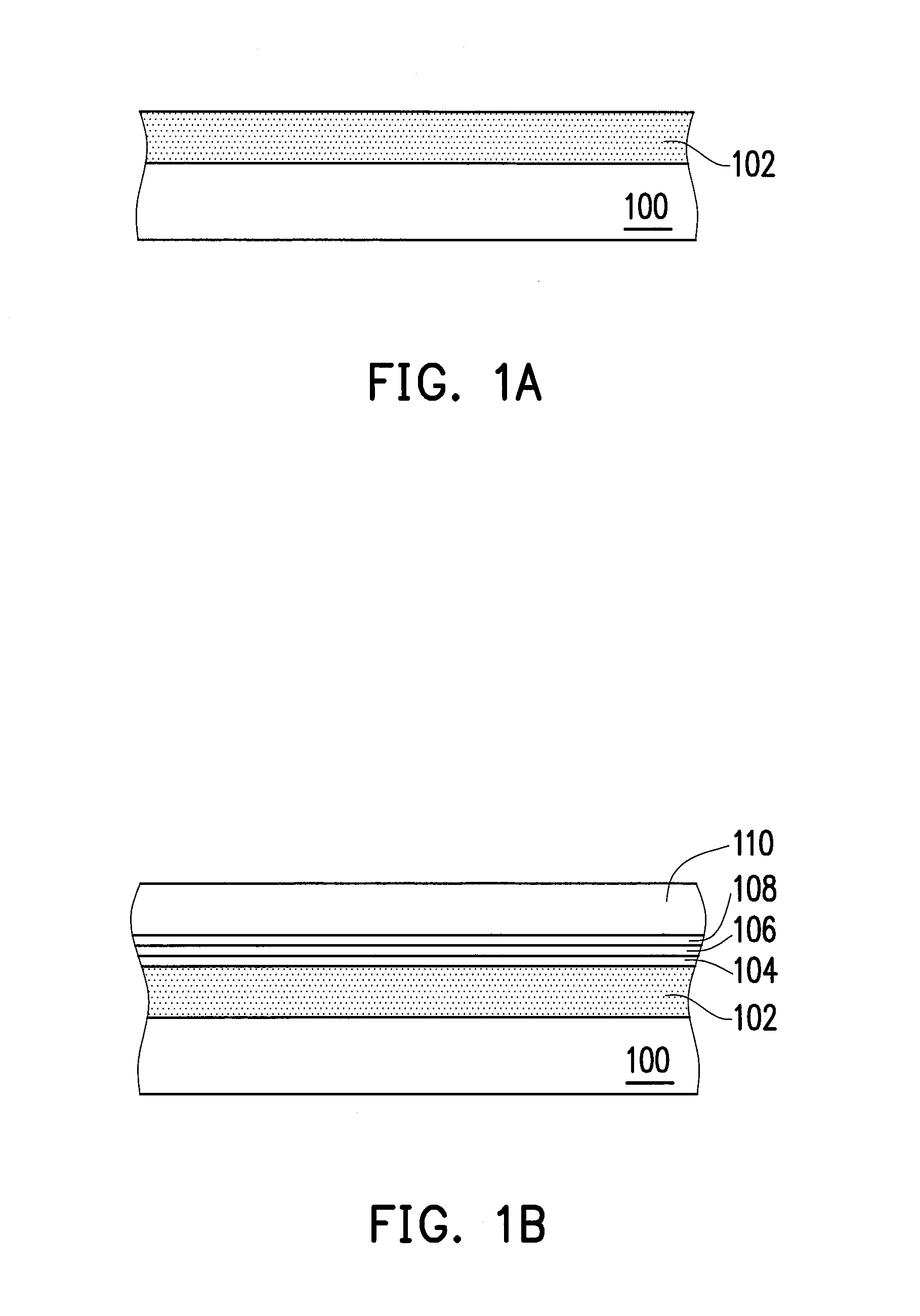
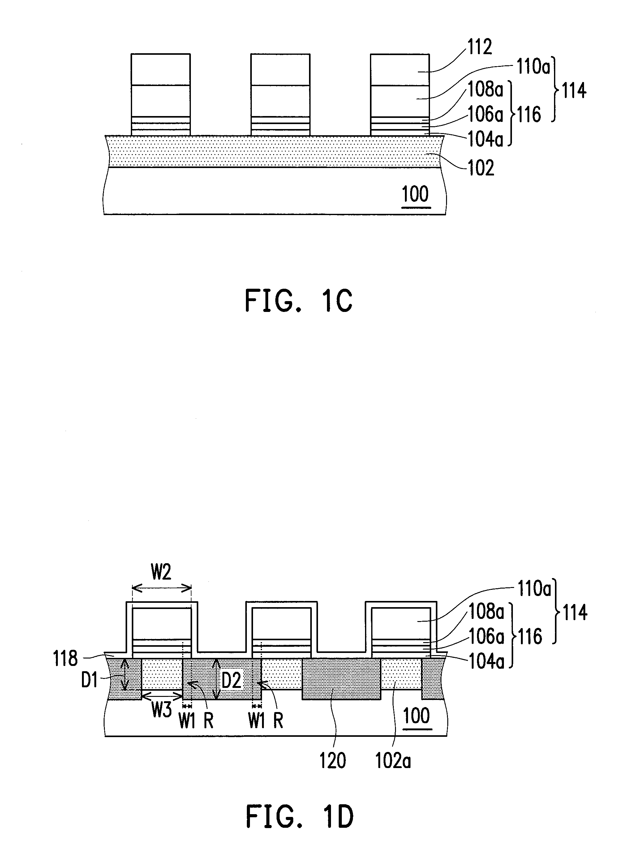
[0035]FIGS. 1A-1E are schematic cross-sectional views illustrating steps of fabricating a non-volatile memory structure according to an embodiment of the invention.
[0036]First, referring to FIG. 1A, a first conductive type doped layer 102 is formed in a substrate 100. The substrate 100 is, for example, a silicon substrate. The first conductive type doped layer 102 may be an N-type doped region or a P-type doped region. A dopant concentration of the first conductive type doped layer 102 is in a range of 1 e18cm−3 to 1 e21cm−3 for example. A dopant depth of the first conductive type doped layer 102 is in a range of 300 Å to 1000 Å, for example. A method for forming the first conductive type doped layer 102 includes an ion implantation method, for example. In this embodiment, the first conductive type doped layer 102 is the N-type doped region, for example, and a dopant used in this embodiment is an N-type dopant, such as As or P.
[0037]Then, referring to FIG. 1B, a dielectric material layer 104, a charge trapping material layer 106, and a dielectric material layer 108 are formed on the substrate 100 sequentially. A material of the dielectric material layer 104 is silicon oxide, for example. A method for forming the dielectric material layer 104 includes a thermal oxidation method, for example. A material of the charge trapping material layer 106 is silicon nitride, for example. A method for forming the charge trapping material layer 106 includes a chemical vapor deposition method, for example. A material of the dielectric material layer 108 is silicon oxide, for example. A method for forming the dielectric material layer 108 is a thermal oxidation method or a chemical vapor deposition method, for example.
[0038]Moreover, a hard mask material layer 110 may be selectively formed on the dielectric material layer 108. A material of the hard mask material layer 110, for example, includes silicon nitride, silicon oxide, or an advanced patterning film (APF) supplied by Applied Materials, Inc. A method for forming the hard mask material layer 110 is, for example, a chemical vapor deposition method.
[0039]Next, referring to FIG. 1C, a patterned photoresist layer 112 is formed on the hard mask material layer 110. A material of the patterned photoresist layer 112 includes a positive type photoresist material or a negative type photoresist material, for example. The patterned photoresist layer 112 may be fabricated by a lithography process.
[0040]Thereafter, the patterned photoresist layer 112 is used as a mask for removing a portion of the hard mask material layer 110, a portion of the dielectric material layer 108, a portion of the charge trapping material layer 106, and a portion of the dielectric material layer 104, so as to form a hard mask layer 110a, a dielectric layer 108a, a charge trapping layer 106a, and a dielectric layer 104a, which form a plurality of stacked structures 114. Each of the stacked structures 114 includes a charge storage structure 116 and may further include the hard mask layer 110a disposed on the charge storage structure 116. The charge storage structure 116 includes the dielectric layer 104a, the charge trapping layer 106a, and the dielectric layer 108a, which are sequentially arranged from the substrate 100. In this embodiment, the stacked structures 114 are formed by patterning the hard mask material layer 110, the dielectric material layer 108, the charge trapping material layer 106, and the dielectric material layer 104. However, a method for forming the stacked structures 114 is not limited to the above.
[0041]Next, referring to FIG. 1D, the patterned photoresist layer 112 is removed. A method for removing the patterned photoresist layer 112, for example, includes a dry photoresist removing method.
[0042]Moreover, a dielectric layer 118 is formed on the substrate 100 between the adjacent stacked structures 114, and the dielectric layer 118 may cover the stacked structures 114. A material of the dielectric layer 118 is silicon oxide, for example. A method for forming the dielectric layer 118 is a thermal oxidation method or a chemical vapor deposition method, for example.
[0043]Thereafter, a second conductive type doped region 120 is formed in the substrate 100 between the adjacent charge storage structures 116. The second conductive type doped region 120 has an overlap region R with each of the charge storage structures 116. In addition, the second conductive type doped region 120 divides the first conductive type doped layer 102 into a plurality of first conductive type doped regions 102a that are separated from each other. The overlap region R of the second conductive type doped region 120 and each of the charge storage structures 116 needs to be sufficient for the charge storage structure 116 located in the overlap region R to function as an effective charge storage region. Moreover, on condition that a program verify condition is met, the size of the overlap region R may be decreased to reduce the second bit effect and program disturbance that are generated during operation. A ratio of a width W1 of the overlap region R of the second conductive type doped region 120 to a width W2 of the charge storage structure 116 is 1:30 to 1:5, for example. In an embodiment, the width W1 of the overlap region R is 30 to 150 Å, for example. A width W3 of the first conductive type doped region 102a is less than the width W2 of the charge storage structure 116, for example.
[0044]In addition, the second conductive type doped region 120 may be an N-type doped region or a P-type doped region. A dopant concentration of the second conductive type doped region 120 is, for example, greater than a dopant concentration of the first conductive type doped region 102a, and a dopant depth D2 of the second conductive type doped region 120 is, for example, greater than a dopant depth D1 of the first conductive type doped region 102a, so as to prevent a punch through phenomenon between the adjacent first conductive type doped regions 102a. The dopant concentration of the second conductive type doped region 120 is in a range of 2 e18cm−3 to 2 e21cm−3 for example. The dopant depth D2 of the second conductive type doped region 120 is in a range of 400 Å to 1100 Å, for example. A method for forming the second conductive type doped region 120 includes using the stacked structures 114 as a mask to perform an ion implantation process, for example. A method for forming the second conductive type doped region 120 in the overlap region R, for example, includes diffusing the dopant into the overlap region R by a thermal process after performing the ion implantation process or directly implanting the dopant into the overlap region R by an inclined-angle ion implantation process. In this embodiment, the second conductive type doped region 120 is the P-type doped region, for example, and the dopant used in this embodiment is a P-type dopant, such as B, BF2, or In.
[0045]In this embodiment, the second conductive type doped region 120 is formed after forming the dielectric layer 118. However, the scope of the invention is not limited thereto. In other embodiments, the second conductive type doped region 120 may also be formed before forming the dielectric layer 118. Since persons skilled in the art can easily carry out the fabrication process with reference to the above embodiments, detailed descriptions are omitted hereinafter.
[0046]Next, referring to FIG. 1E, a conductive layer 122 is formed on the dielectric layer 118. A material of the conductive layer 122 is doped polysilicon or metal, for example. A method for forming the conductive layer 122 is, for example, a chemical vapor deposition method.
[0047]It can be known from the above embodiments that, in the non-volatile memory structure, the charge storage structures 116 used for storing charges are located at two sides of the second conductive type doped region 120 and are separated from each other, and most of the programmed charge distribution is restricted within the charge storage structures 116 in the overlap region R. Consequently, the second bit effect and program disturbance that are generated during operation may be reduced. Hence, the fabricating method, disclosed in the above embodiments, is applicable to fabricating a non-volatile memory that has better performance and reliability.
[0048]Hereinafter, a memory structure according to an embodiment of the invention is described with reference to FIG. 1E.
[0049]The non-volatile memory structure includes the substrate 100, the plurality of stacked structures 114, the plurality of first conductive type doped regions 102a, at least one second conductive type doped region 120, the conductive layer 122, and the dielectric layer 118. The stacked structures 114 are disposed on the substrate 100. Each of the stacked structures 114 includes the charge storage structure 116 and may further include the hard mask layer 110a disposed on the charge storage structure 116. Each of the charge storage structures 116 includes the dielectric layer 104a, the charge trapping layer 106a, and the dielectric layer 108a, which are sequentially arranged from the substrate 100. The first conductive type doped regions 102a are disposed in the substrate 100 under the corresponding charge storage structures 116 respectively. The second conductive type doped region 120 is disposed in the substrate 100 between the adjacent charge storage structures 116 and has the overlap region R with each of the charge storage structures 116. The conductive layer 122 covers the second conductive type doped region 120 and may further cover the stacked structures 114. The dielectric layer 118 is disposed between the conductive layer 122 and the second conductive type doped region 120 and may be further disposed between the stacked structures 114 and the conductive layer 122. The materials, forming methods, proportions, and efficiency of the elements of the non-volatile memory structure have been described in detail in the above embodiments and thus shall not be repeated hereinafter.
[0050]In a memory cell 124, the second conductive type doped region 120 may serve as a channel region. The first conductive type doped regions 102a located at two sides of the second conductive type doped region 120 may serve as a source region or a drain region. The charge trapping layers 106a in the charge storage structures 116 located at two sides of the second conductive type doped region 120 may be used for trapping charges and form a first bit and a second bit of the memory cell 124.
[0051]It can be known from the above embodiments that, when performing a programming operation on the memory cell 124, charges from the first conductive type doped region 102a at one side of the second conductive type doped region 120 are injected into the charge storage structure 116 at the other side of the second conductive type doped region 120 through the channel formed by the second conductive type doped region 120. In the memory cell 124, the charge storage structures 116 used for storing charges are located at two sides of the second conductive type doped region 120 and are separated from each other, and most of the programmed charge distribution is restricted within the charge storage structures 116 in the overlap region R. Consequently, the non-volatile memory structure disclosed in the embodiments can be conducive to reducing the second bit effect and program disturbance that are generated during operation. In addition, although the programming charges may be injected into the charge storage structures 116 above the first conductive type doped regions 102a, the charges in the charge storage structures 116 above the first conductive type doped regions 102a do not cause an initiation voltage (Vt) of a reading operation to vary and thus do not worsen the second bit effect.
[0052]To conclude the above, the above embodiments at least have the following characteristics. The non-volatile memory structure disclosed in the above embodiments can be conducive to reducing the second bit effect and program disturbance that are generated during operation. Moreover, the fabricating method of the non-volatile memory structure disclosed in the above embodiments is applicable to fabricating a non-volatile memory that has better performance and reliability.
[0053]It will be apparent to those skilled in the art that various modifications and variations can be made to the disclosed embodiments without departing from the scope or spirit of the invention. In view of the foregoing, it is intended that the invention covers modifications and variations of this disclosure provided that they fall within the scope of the following claims and their equivalents.

PUM

no PUM

Description & Claims & Application Information

We can also present the details of the Description, Claims and Application information to help users get a comprehensive understanding of the technical details of the patent, such as background art, summary of invention, brief description of drawings, description of embodiments, and other original content. On the other hand, users can also determine the specific scope of protection of the technology through the list of claims; as well as understand the changes in the life cycle of the technology with the presentation of the patent timeline. Login to view more.
Why Eureka
Try Eureka