Liquid crystal display device

a liquid crystal display and display device technology, applied in non-linear optics, instruments, optics, etc., can solve the problems of reducing the use efficiency of backlight, unsuitable for higher definition, and complicated pixels of eight-domain displays, so as to achieve less whitening and tinting

Inactive Publication Date: 2014-11-20
FUJIFILM CORP
View PDF3 Cites 7 Cited by
  • Summary
  • Abstract
  • Description
  • Claims
  • Application Information

AI Technical Summary

Benefits of technology

[0044]The invention can achieve a VA-mode liquid crystal display device of four domains or less that causes less whitening and tinting.

Problems solved by technology

However, the eight-domain display has a complicated pixel structure, which is unsuitable for higher definition.
Furthermore, the higher definition leads to a decrease in the use efficiency of the backlight.
However, a reduced number of domains leads to whitening of images (displayed images appear brighter when viewed from the side).

Method used


Image

  • Liquid crystal display device
  • Liquid crystal display device
  • Liquid crystal display device

Examples


first embodiment

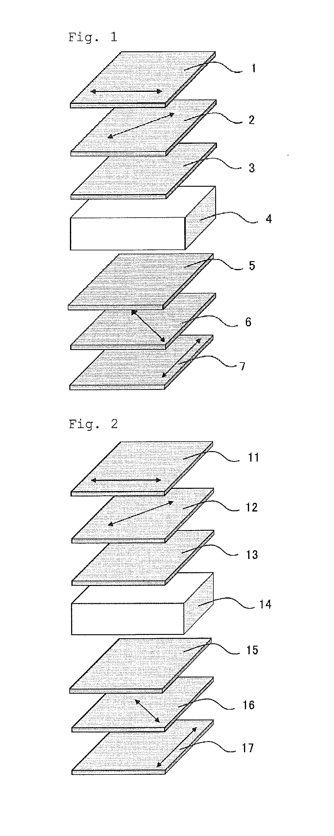
[0065]FIG. 3 illustrates an example structure of a liquid crystal display device according to the first embodiment of the invention. The device includes a first polarizing film, a first retardation layer, a second retardation layer, a liquid crystal layer, a third retardation layer, a fourth retardation layer, and a second polarizing film, in sequence. The liquid crystal layer has four domains or less, and is in a vertical alignment mode (VA mode) under no voltage application. The first and fourth retardation layers each have an in-plane retardation Re (550) of 25 to 125 nm at a wavelength of 550 nm, and have a thickness retardation Rth (550) of 12.5 to 62.5 nm at a wavelength of 550 nm. The absolute value of the retardation Re (550) of the second retardation layer is 10 nm or smaller, while the retardation Rth (550) of the second retardation layer is −200 to −100 nm. The absolute value of the retardation Re (550) of the third retardation layer is 10 nm or smaller, while the retarda...

second embodiment

[0103]FIG. 4 illustrates an example structure of a liquid crystal display device according to the second embodiment of the invention. The device includes a first polarizing film, a first retardation layer, a second retardation layer, a liquid crystal layer, a third retardation layer, a fourth retardation layer, and a second polarizing film, in sequence. The liquid crystal layer has four domains or less, and is in a vertical alignment mode (VA mode) under no voltage application. The first and fourth retardation layers each have an in-plane retardation Re (550) of 25 to 125 nm at a wavelength of 550 nm, and have a thickness retardation Rth (550) of 12.5 to 62.5 nm at a wavelength of 550 nm. The absolute value of the retardation Re (550) of the second retardation layer is 10 nm or less, while the retardation Rth (550) of the second retardation layer is −300 to −200 nm. The absolute value of the retardation Re (550) of the third retardation layer is 10 nm or less, while the retardation ...

third embodiment

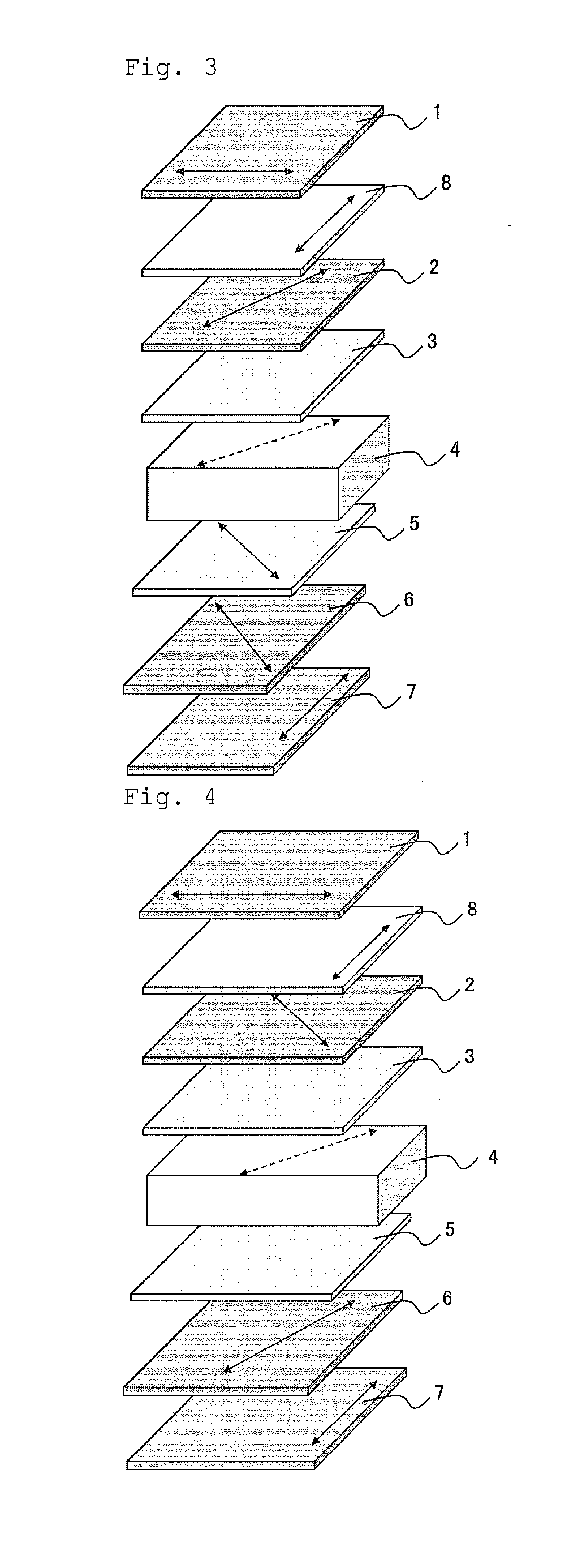
[0125]FIG. 3 illustrates an example structure of a liquid crystal display device according to the third embodiment of the invention. The device includes a first polarizing film, a first retardation layer, a second retardation layer, a liquid crystal layer, a third retardation layer, a fourth retardation layer, and a second polarizing film, in sequence. The liquid crystal layer has four domains or less, and is in a vertical alignment mode (VA mode) under no voltage application. The first and fourth retardation layers each have an in-plane retardation Re (550) of 25 to 125 nm at a wavelength of 550 nm, and have a thickness retardation Rth (550) of −62.5 to −12.5 nm at a wavelength of 550 nm. The absolute value of the retardation Re (550) of the second retardation layer is 10 nm or less, while the retardation Rth (550) of the second retardation layer is −150 to −50 nm. The absolute value of the retardation Re (550) of the third retardation layer is 10 nm or less, while the retardation ...


PUM

PropertyMeasurementUnit
thickness retardation Rth (aaaaaaaaaa

Abstract

A VA-mode liquid crystal display device of four domains or less that causes less whitening and tinting, includes: a first polarizing film, a first retardation layer, a second retardation layer, a liquid crystal layer, a third retardation layer, a fourth retardation layer, and a second polarizing film, in sequence. The liquid crystal layer is in a vertical alignment mode (VA mode) under no voltage application. The first to fourth retardation layers each have a predetermined retardation. The absorption axis of the first polarizing film is orthogonal to that of the second polarizing film. The slow axis of the first retardation layer defines an angle of 45° from the absorption axis of the first polarizing film, and is parallel to the in-plane slow axis of the liquid crystal layer under voltage application. The slow axis of the first retardation layer is orthogonal to that of the fourth retardation layer.

Description

CROSS-REFERENCE TO RELATED APPLICATIONS[0001]The present application claims the benefit of priority from Japanese Patent Application No. 105645 / 2013, filed on May 17, 2013, the contents of which are herein incorporated by reference in their entirety.TECHNICAL FIELD[0002]The present invention relates to a liquid crystal display device.BACKGROUND ART[0003]In the recent flat-panel display market, higher definition pixels have been pursued to improve the image quality. The progress in compact displays such as tablet PCs and smartphones is particularly remarkable. In addition, high definition televisions called 4K2K are also appearing on the market.[0004]Among known liquid crystal modes including a TN mode, an IPS mode, and a VA mode, the VA mode is dominant in televisions. Most of the current VA modes employ a pixel division scheme called eight domains (8D).[0005]However, the eight-domain display has a complicated pixel structure, which is unsuitable for higher definition. Furthermore, ...

Claims


Application Information

Patent Timeline
Patent Type & Authority Applications(United States)
IPC IPC(8): G02F1/1335
CPCG02F1/1335G02F1/133634G02F2413/04G02F2413/06G02F1/13712
Inventor YANAI, YUJIROSAITOH, YUKITOSATO, HIROSHI
Owner FUJIFILM CORP
Why Eureka
Try Eureka