Compact Optical Waveguide Arrays and Optical Waveguide Spirals

a technology of optical waveguide array and optical waveguide spiral, which is applied in the field of optical waveguides, can solve the problems of limiting the density of optical waveguides on a chip, limiting layout flexibility and/or connectivity space requirements on the chip, and chips having a large number of devices

Inactive Publication Date: 2015-02-19
HUAWEI TECH CO LTD
View PDF4 Cites 150 Cited by
  • Summary
  • Abstract
  • Description
  • Claims
  • Application Information

AI Technical Summary

Benefits of technology

[0005]In accordance with an embodiment, an apparatus for housing optical waveguides is provided. In this example, the apparatus includes a substrate layer and a waveguide bundle. The waveguide bundle includes a plurality of waveguides extending across the substrate layer. The waveguides run parallel to one another and include waveguides having three or more different widths.

Problems solved by technology

Notably, optical waveguides typically generate crosstalk when placed in close proximity, which may limit the density of optical waveguides on a chip as well as constrain layout flexibility and / or connectivity space requirements on the chip.
In other words, chips having large number of devices may need to devote a substantial area on the chip for optical waveguide routing.
The efficiency of spiral thermo-optic devices in relation to heat exchangers is also limited by the compactness of optical waveguide spirals.

Method used


Image

  • Compact Optical Waveguide Arrays and Optical Waveguide Spirals
  • Compact Optical Waveguide Arrays and Optical Waveguide Spirals
  • Compact Optical Waveguide Arrays and Optical Waveguide Spirals

Examples


Embodiment Construction

[0021]The making and using of embodiments of this disclosure are discussed in detail below. It should be appreciated, however, that the present disclosure provides many applicable inventive concepts that can be embodied in a wide variety of specific contexts. The specific embodiments discussed are merely illustrative of specific ways to make and use the invention, and do not limit the scope of the claimed invention.

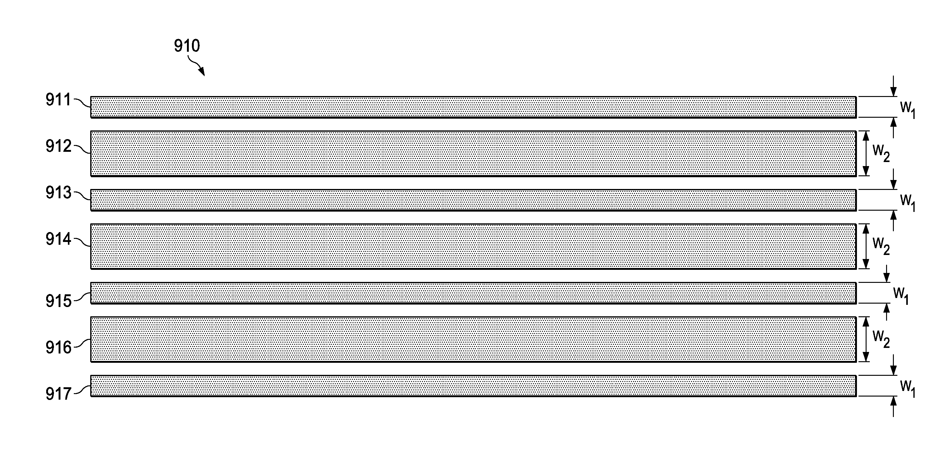
[0022]Conventional waveguide bundles may typically consist of waveguides having identical widths. Aspects of this disclosure reduce crosstalk in optical waveguide bundles by varying the widths of the individual waveguides. More specifically, using different width waveguides reduces the growth of crosstalk between the optical waveguides, thereby allowing the waveguides to be placed in closer proximity to increase waveguide density on the chip and / or reduce the routing space required for the waveguide bundle. Accordingly, embodiments of this disclosure achieve more flexible...


PUM


Abstract

Crosstalk can be reduced in optical waveguide bundles by varying the widths of individual waveguides. Using different width waveguides reduces the growth of crosstalk between the optical waveguides, thereby allowing the waveguides to be placed in closer proximity to increase waveguide density on the chip and/or reduce the routing space required for the waveguide bundle. Moreover, varying the width of a waveguide spiral may reduce crosstalk, which can increase power efficiency when implemented in coiled or folded waveguide thermal optical (TO) devices.

Description

[0001]This application claims the benefit of U.S. Provisional Application No. 61 / 865,499 filed on Aug. 13, 2013, entitled “Compact Optical Waveguide Arrays and Optical Waveguide Spirals,” which is incorporated herein by reference as if reproduced in its entirety.TECHNICAL FIELD[0002]The present invention relates to optical waveguides, and, in particular embodiments, to compact optical waveguide arrays and optical waveguide spirals.BACKGROUND[0003]Optical waveguides are physical structures that guide electromagnetic waves in the optical spectrum, and are often bundled together in order to route multiple signals in-between components of an integrated circuit. Notably, optical waveguides typically generate crosstalk when placed in close proximity, which may limit the density of optical waveguides on a chip as well as constrain layout flexibility and / or connectivity space requirements on the chip. In other words, chips having large number of devices may need to devote a substantial area...

Claims


Application Information

Patent Timeline
Patent Type & Authority Applications(United States)
IPC IPC(8): G02B6/04
CPCG02B6/04G02B6/12011
Inventor DUMAIS, PATRICK
Owner HUAWEI TECH CO LTD
Why Eureka
Try Eureka