Micro-fabricated optical waveguide for use in scanning fiber displays and scanned fiber image acquisition

a micro-fabricated, optical waveguide technology, applied in the direction of optics, optical light guides, instruments, etc., can solve the problems of mirror surface, degrading image quality, limiting the application of optical scanning for small size, etc., and achieve the effect of flattening the ar

Inactive Publication Date: 2005-02-15
UNIV OF WASHINGTON +1
View PDF28 Cites 339 Cited by
  • Summary
  • Abstract
  • Description
  • Claims
  • Application Information

AI Technical Summary

Benefits of technology

The scanner may further include a linear actuator that is coupled to the control circuit. The linear actuator periodically varies a force applied to the waveguide that is directed generally along the longitudinal axis of the waveguide

Problems solved by technology

Combining both high resolution (>400,000 pixels) and wide FOV (>30°) in a single display is a difficult technical challenge, limiting the application of optical scanning for small size, low cost optical scanners that have both high-resolution and wide FOV.
The faster the mirror scans, the greater the forces acting on the mirror, which deforms the mirror surface, degrading image quality.
This limitation is especially true for the small, low cost resonant mirror scanners.
Rotating polygon mirror scanners can overcome this limitation or tradeoff between scan frequency and amplitude, except they are usually bulky, noisy, and costly.
However, at sVGA resolution and scan frequencies, optical FOVs on the order of 30° to 60° cannot be achieved using a low cost resonant mirror scanner as the basis for micro displays.
Nonetheless, there is still a tradeoff between scan amplitude and scan frequency of t

Method used


Image

  • Micro-fabricated optical waveguide for use in scanning fiber displays and scanned fiber image acquisition
  • Micro-fabricated optical waveguide for use in scanning fiber displays and scanned fiber image acquisition
  • Micro-fabricated optical waveguide for use in scanning fiber displays and scanned fiber image acquisition

Examples


second embodiment

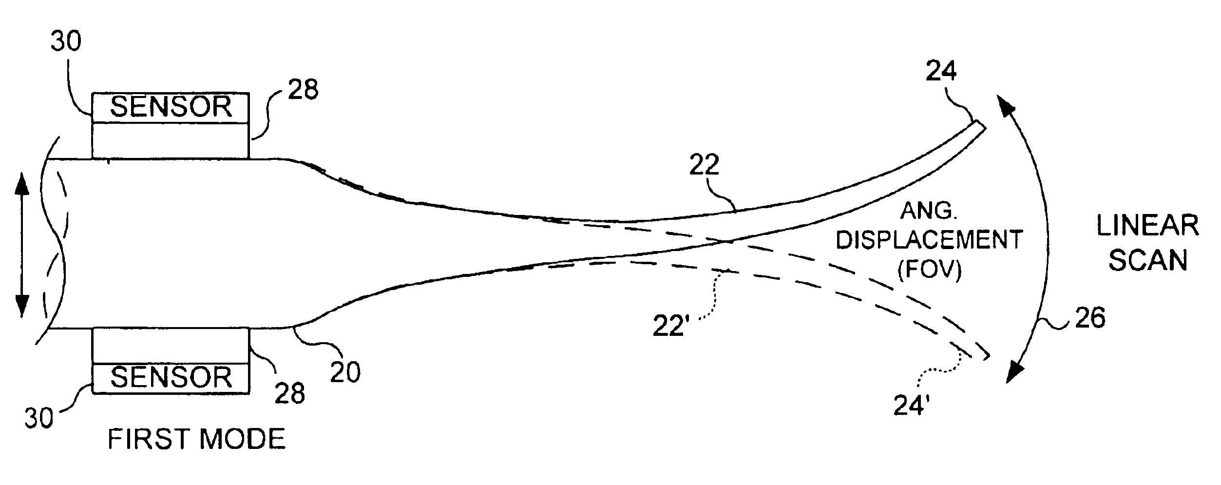
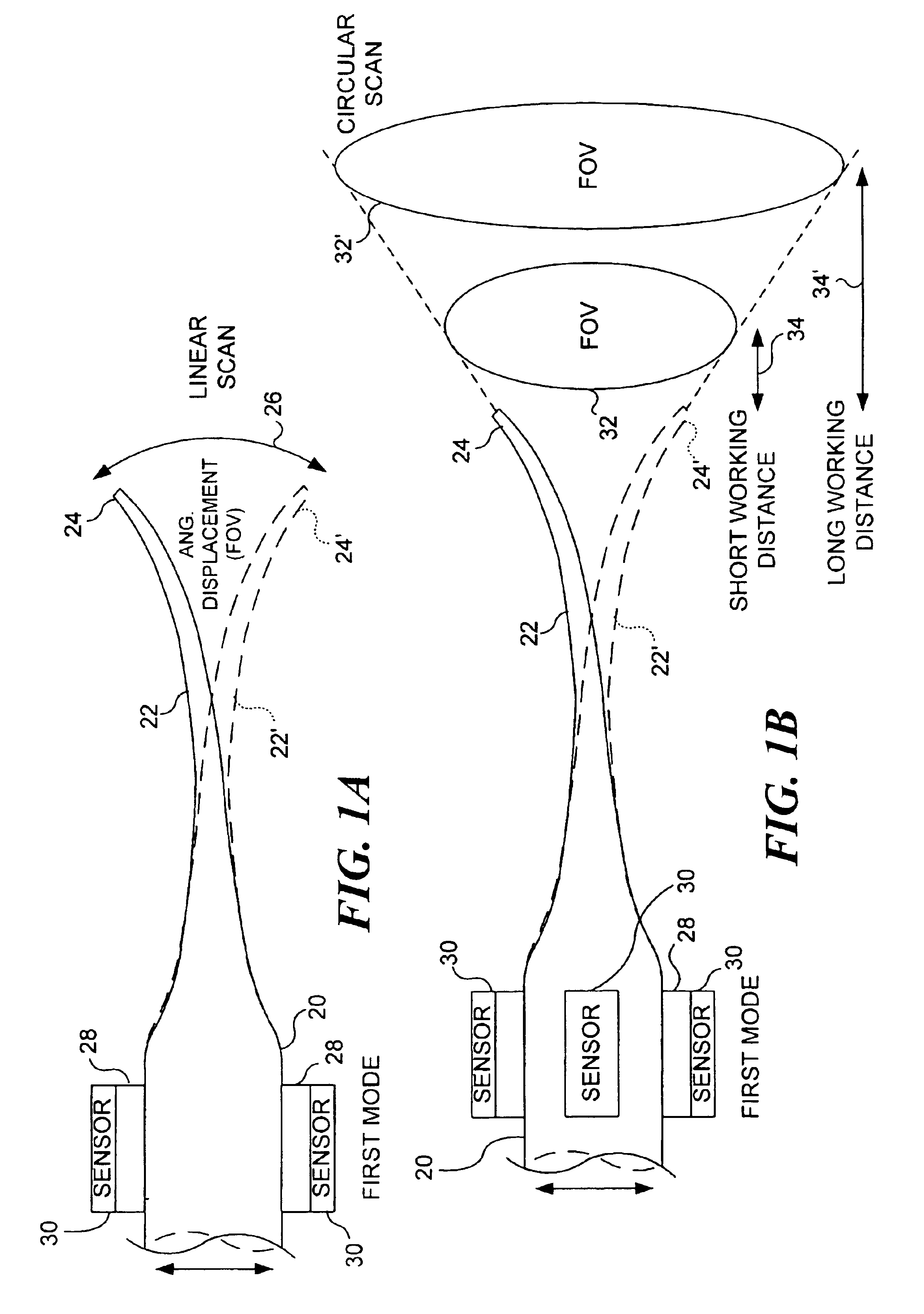
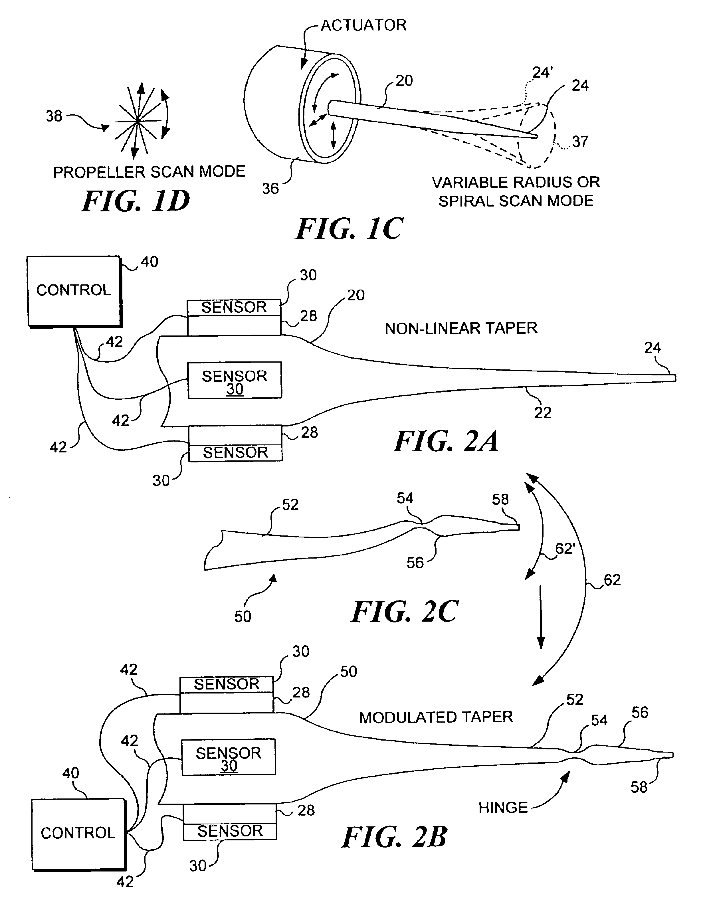
A second embodiment employs an optical source producing radiation at a wavelength not being used for the scanner application (e.g., infrared (IR) lasers or light emitting diodes (LEDs)) and matching IR detectors (IR photodiodes) to monitor the direction of the scanning waveguide. Sensors 30 in FIGS. 1A, 1B, 2A, and 2B correspond to these optical sensors in this embodiment. Details of exemplary sensors suitable for this purpose are disclosed in the priority parent patent application referenced above. Both the light sources and detectors are preferably made from diode material that can be positioned at either the distal or proximal end or the micro-fabricated fiber scanner. If the diode material is disposed at the proximal end, then the diodes will send and receive light to and from the distal tip using optical fibers running with the scanning optical waveguide. If disposed instead at the distal end, then the diodes may be positioned to detect an IR beam (or other waveband of light th...


PUM


Abstract

Small, rugged scanners micro-fabricated from commercial optical fibers to form waveguides or other structures. The scanning waveguide has a distal portion on which is formed a non-linear taper with a diameter that decreases toward a distal end. Optionally, a hinge portion having a reduced diameter can be formed in the distal portion, improving the scanning properties of the waveguide. A micro-lens can be integrally formed at the distal tip of the waveguide with either a droplet of an optical adhesive, or by using an energy beam to melt the material of the waveguide to form a droplet. The droplet is shaped with an externally applied force. When mechanically driven in vibratory resonance, the tip of the optical waveguides moves in linear or two-dimensional scan patterns of relatively high amplitude and frequency, and large field of view. The scanner can be used either for image acquisition or image display.

Description

FIELD OF THE INVENTIONThe present invention generally relates to optical fiber scanners, and more specifically, to a micro-fabricated optical fiber that is driven at resonance to scan a relatively large field of view.BACKGROUND OF THE INVENTIONMost optical scanning applications use a moving mirror, either rotating or oscillating. A laser beam is often projected onto the moving mirror to scan the beam across a specified linear or two-dimensional (2D) (raster) pattern at a frequency that is sufficient for the particular application. For optical displays, the field of view (FOV) is determined by the scanning amplitude and the particular optical design. There is a minimum frequency (rate) at which scanning displays need to be refreshed, which is determined by the human perception of flicker from a scanned display. For ubiquitous raster scanning displays, such as cathode ray tubes (CRTs) used in televisions and computer monitors, the display refresh rate is typically 30 to 60 Hz. Althoug...

Claims


Application Information

Patent Timeline
IPC IPC(8): G02B26/10G02B6/26G02B6/35G02B6/32
CPCG02B6/241G02B6/245G02B6/25G02B26/10G02B6/3502G02B6/262G02B6/32G02B6/3586
Inventor FAUVER, MARK E.SEIBEL, ERIC J.BROWN, CHRIS M.REINHALL, PER G.SMITHWICK, QUINN Y. J.
Owner UNIV OF WASHINGTON
Why Eureka
Try Eureka