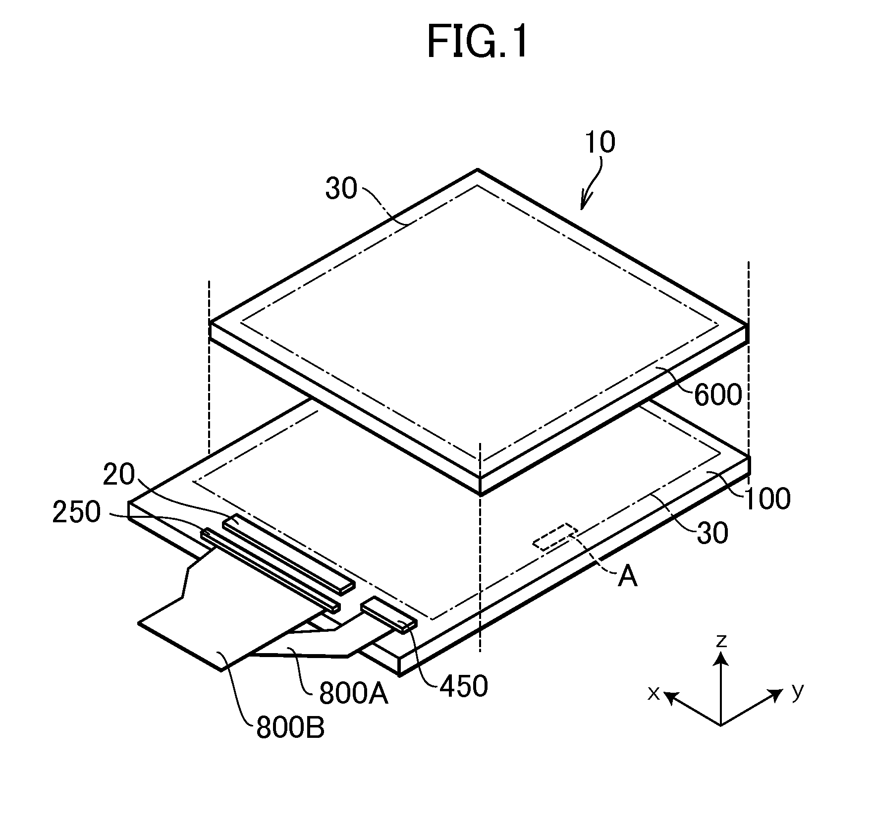
Display device

Active Publication Date: 2015-03-05
JAPAN DISPLAY INC
View PDF12 Cites 72 Cited by
  • Summary
  • Abstract
  • Description
  • Claims
  • Application Information

AI Technical Summary

Benefits of technology

[0015]Also, the planarizing layer may have a thickness of 1 to 100 μm. Also, a connection terminal for connection with the touch sensor control unit, and a connection terminal

Problems solved by technology

However, the display device with the touch sensor in which the touch panel is adhered to the surface of the display screen as another member, or provides the touch sensor function in a part of the counter su

Method used


Image

  • Display device
  • Display device
  • Display device

Examples


first embodiment

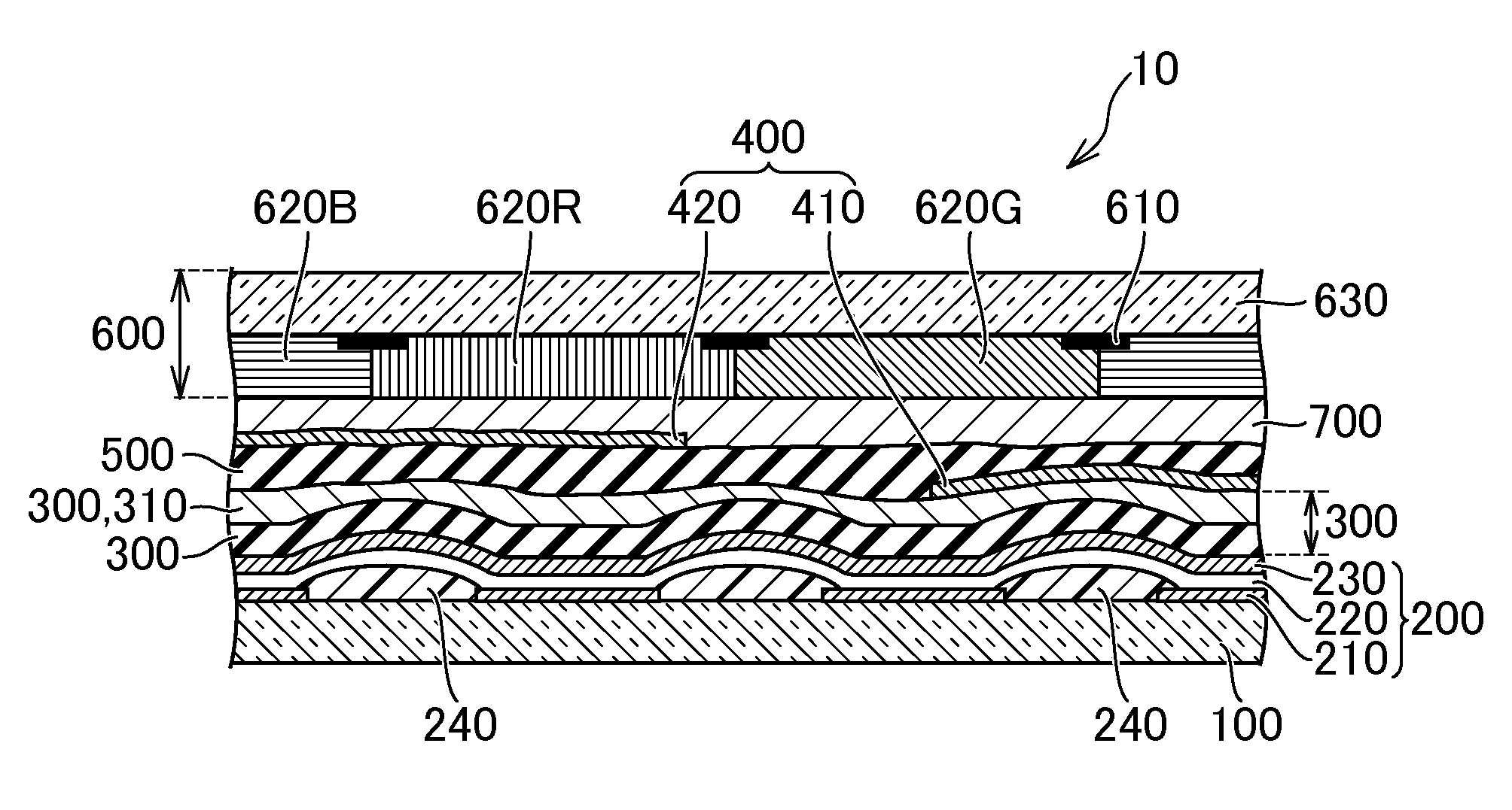
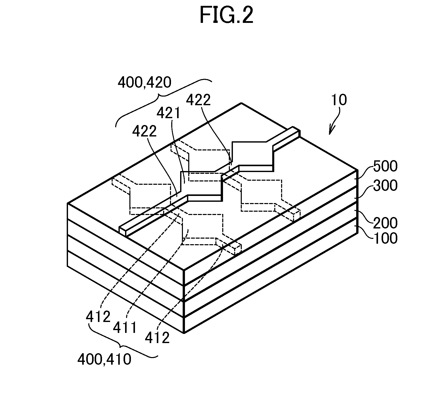
[0026]According to the first embodiment of the present invention, there is provided a display device, including: a first substrate in which pixels each having a thin-film transistor are arranged in a matrix on an insulating substrate; a second substrate that is arranged opposite to the first substrate; an organic EL element layer that is arranged on the first substrate and between the first substrate and the second substrate, and emits light under control by a circuit including the thin film transistor; a first sealing film which is arranged on a side of the organic EL element layer opposite to the second substrate side, and covers the organic EL element layer; a plurality of first detection electrodes that extend in one direction, and are arranged in parallel in a partial area on a side of the first sealing film opposite to the second substrate; a second sealing film that is arranged to cover another area that is an outside of the partial area in which the first detection electrode...

second embodiment

[0080]Hereinafter, a description will be given an embodiment in which even if a higher-definition organic electroluminescent display unit is applied to the organic electroluminescent device with a touch sensor 10, the disconnection of the detection electrodes configuring the touch sensor is suppressed while thinning the device.

[0081]An organic electroluminescent device with a touch sensor 10 according to a second embodiment of the present invention is different from the organic electroluminescent device with a touch sensor 10 according to the first embodiment in that the first sealing film 300 is configured by the first sealing film 300 and a first planarizing layer 310.

[0082]FIG. 4B is a cross-sectional view of the organic electroluminescent device with a touch sensor 10 according to the second embodiment of the present invention. As illustrated in FIG. 4B, the first sealing film 300 of the organic electroluminescent device with a touch sensor 10 according to the second embodiment ...


PUM


Abstract

An organic electroluminescent device with a touch sensor including: a first substrate; a second substrate arranged opposite to the first substrate; an organic EL element layer arranged above the first substrate; a first sealing film arranged toward the second substrate of the organic EL element layer, covering the organic EL element layer, and including a first inorganic layer; plural first detection electrodes extending in one direction, and arranged in parallel toward the second substrate of the first sealing film; a second sealing film arranged toward the second substrate of the first detection electrodes, and including a second inorganic layer; plural second detection electrodes extending in another direction different from the one direction, and arranged in parallel toward the second substrate of the second sealing film; and a touch sensor control unit controlling a potential to detect a touch with a display surface.

Description

CROSS-REFERENCE TO RELATED APPLICATION[0001]The present application claims priority from Japanese patent application JP2013-179505 filed on Aug. 30, 2013, the content of which is hereby incorporated by reference into this application.BACKGROUND OF THE INVENTION[0002]1. Field of the Invention[0003]The present invention relates to a display device.[0004]2. Description of the Related Art[0005]JP-2012-156140 A discloses an organic light emitting display device including: a substrate; a display part that is formed on the substrate; a sealing substrate having a surface that faces the substrate; a capacitance type touch unit having plural first sensors that are formed on any surface of the sealing substrate to be aligned along a first direction, and plural second sensors that are formed to be aligned in a second direction intersecting the first direction; and an insulating layer that is formed on at least a part of the first sensor and the second sensor, in which the first sensors and the ...

Claims


Application Information

Patent Timeline
IPC IPC(8): H01L27/32
CPCH01L27/323H01L27/3253G06F3/0445G06F3/0446H10K59/40H05K1/118H10K59/131H10K50/805H10K50/844G06F3/044H10K50/822H10K50/8426H10K59/1275
Inventor SATO, TOSHIHIROITO, RYOICHI
Owner JAPAN DISPLAY INC
Why Eureka
Try Eureka