Unlock instant, AI-driven research and patent intelligence for your innovation.

Interconnect system

a technology of interconnection system and connector, which is applied in the manufacture of printed circuits, printed circuit aspects, basic electric elements, etc., can solve the problems of affecting the functionality of semiconductors, affecting the performance of semiconductors, etc., and achieves high electrical conductivity and high conductivity.

Inactive Publication Date: 2015-04-09
HARRIS JAMES M
View PDF1 Cites 7 Cited by
  • Summary
  • Abstract
  • Description
  • Claims
  • Application Information

AI Technical Summary

Benefits of technology

The invention is a new process for making high-conductivity electrical contacts to semiconductors or other metallization systems without the need for a barrier layer between the contact metallization and the semiconductor surface. This is achieved by using a contact transition metal layer and a layer of graphene, Cg, which replaces copper or gold and eliminates the need for a barrier layer. The technical effect is a more efficient and reliable method for creating high-conductivity electrical contacts.

Problems solved by technology

Copper is deleterious to semiconductor functionality and must be prevented from migrating to a semiconductor.

Method used


Image

  • Interconnect system
  • Interconnect system
  • Interconnect system

Examples


Embodiment Construction

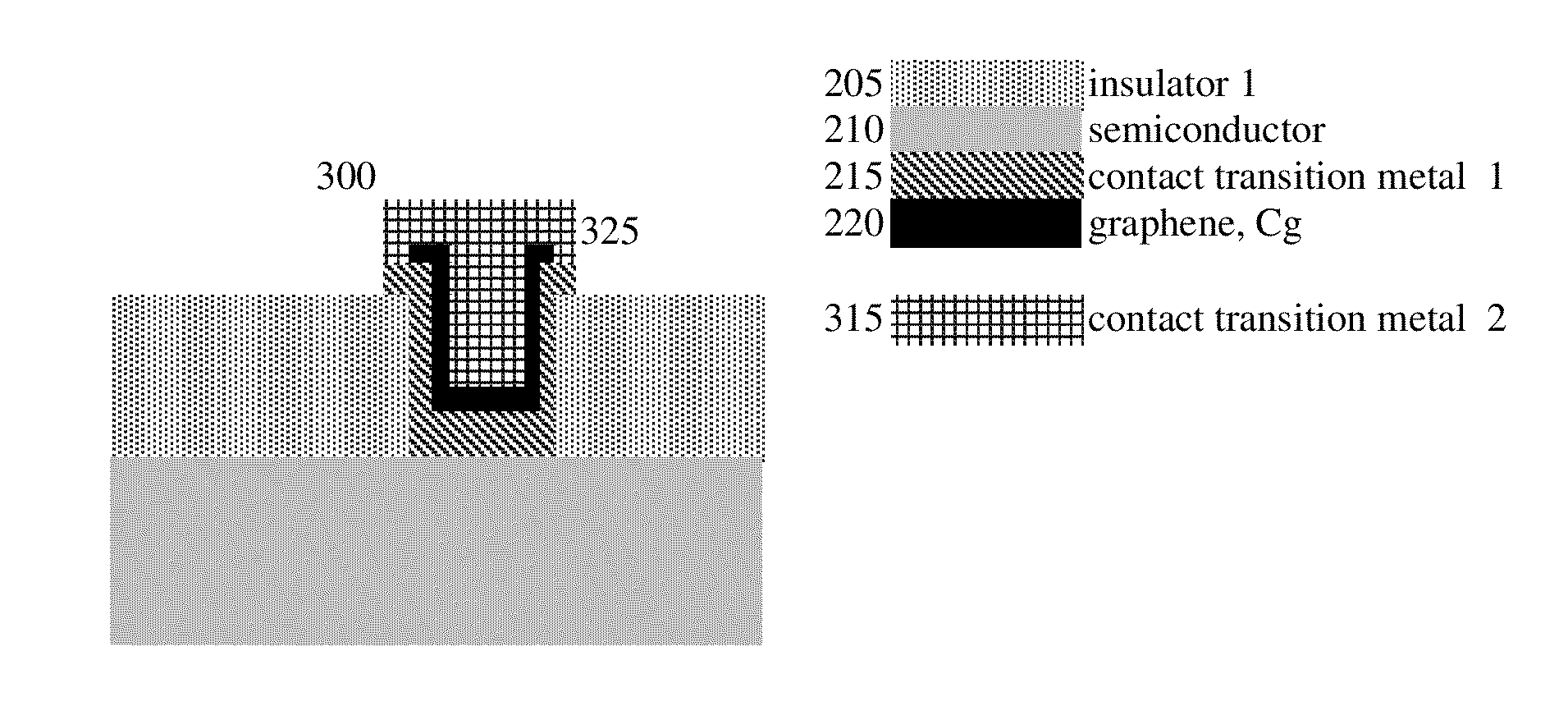
[0012]One embodiment of the instant invention relates to forming electrical contact to a semiconductor surface using a “contact transition metal”. Currently a silicide and / or barrier layer must be formed in a via to prevent migration of copper into the semiconductor; as shown in FIG. 1. In some embodiments a barrier layer is not required in the instant invention. In the case of Si, Ge or Si / Ge contact to a semiconductor is made through the use of a transition metal such as Ti, Cr, Co, Ni, Pd, Ta, W, Os, Ir, and Pt; these metals can also serve as a catalytically enhanced surface for deposition of a graphene, Cg, film or layer. As one knowledgeable in the art knows not all transition metals are functional with all Group II, III, IV, V and VI semiconductors; one must select specific transition metals for specific semiconductors or specific semiconductor groupings; a transition metal grouping specific to a predetermined class of semiconductors is termed “contact transition metal(s)”. In...


PUM


Abstract

An electrical contact and electrical interconnect network comprising graphene and a transition metal for a solid state device and an interconnect network for a circuit board or substrate are disclosed.

Description

PRIORITY[0001]This application claims priority form U.S. Ser. No. 61 / 887,145; filed on Oct. 4, 2013; incorporated herein in its entirety.BACKGROUND OF THE INVENTION[0002]1. Field of Invention[0003]The invention relates generally to solid state device manufacturing processes and associated packaging techniques. In particular, the invention relates to improved methods of forming an electrical contact to a semiconductor, forming an electrical interconnect network and a method for patterning an interconnect network on a circuit board or substrate.[0004]2. Description of Background Art[0005]A critical step in the manufacture of all solid state devices is making electrical contact to a semiconductor surface and / or electrical conductor providing electrical continuity between various components. Current practice in state-of-the-art devices is to use a copper metallization system. Copper is deleterious to semiconductor functionality and must be prevented from migrating to a semiconductor. Cu...

Claims


Application Information

Patent Timeline
Patent Type & Authority Applications(United States)
IPC IPC(8): H01L23/532H01L29/872H01L29/45
CPCH01L23/53276H01L23/53209H01L29/872H01L29/45H01L29/401H01L29/452H01L29/1606H01L2924/0002H01L23/49877H01L23/485H01L23/53257H05K3/421H05K2201/0323H01L2924/00
Inventor HARRIS, JAMES M.
Owner HARRIS JAMES M