Metrology Optimized Inspection

Active Publication Date: 2015-05-07
KLA TENCOR CORP
View PDF21 Cites 9 Cited by
  • Summary
  • Abstract
  • Description
  • Claims
  • Application Information

AI Technical Summary

Benefits of technology

The patent describes a method for determining parameters for a wafer inspection process using metrology data from a wafer metrology system. The method involves acquiring the data and then determining the parameters of the inspection process based on the data. The resulting system can be computer software or a computer system with an inspection subsystem and a computer subsystem. The technical effect is to improve the accuracy and efficiency of the wafer inspection process by utilizing metrology data to optimize the inspection process parameters.

Problems solved by technology

For instance, as the dimensions of semiconductor devices decrease, detection of defects of decreasing size has become necessary since even relatively small defects may cause unwanted aberrations in the semiconductor devices.
Although an inspection system that has adjustable output acquisition and sensitivity parameters presents significant advantages to a semiconductor device manufacturer, these inspection systems are essentially useless if the incorrect output acquisition and sensitivity parameters are used for an inspection process.
Although using the correct output acquisition and sensitivity parameters will have a dramatic effect on the results of inspection, it is conceivable that many inspection processes are currently being performed with incorrect or non-optimized output acquisition and sensitivity parameters.
In such applications, a user can guess the best place to collect data but that place may not represent true nominal conditions.
In the area of inspection optimization, not knowing where the noisy areas are can result in setting up sensitivity based on only noisy regions or only quiet regions that may not truly reflect variations across wafers.
If die row selection was done on a quiet region, additional nuisance defects may arise when additional wafers are scanned.
If die selection was done in a noisy region, real defects may be missed during production wafer scans due to thresholds being set too high.
With respect to nominal die selection, the challenge is to select dies that are at truly nominal conditions where average thickness, critical dimension (CD), etc. are present.
Not having this data set can lead to selecting dies that do not represent the nominal signature.
With regard to defect sampling, defects that are sampled in a noisy region can produce low signal-to-noise while an optimized sampling from a quiet region may yield more real defects.

Method used


Image

  • Metrology Optimized Inspection
  • Metrology Optimized Inspection

Examples


Embodiment Construction

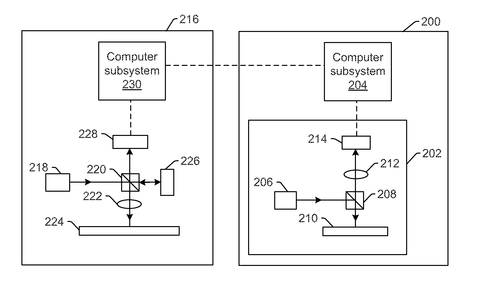
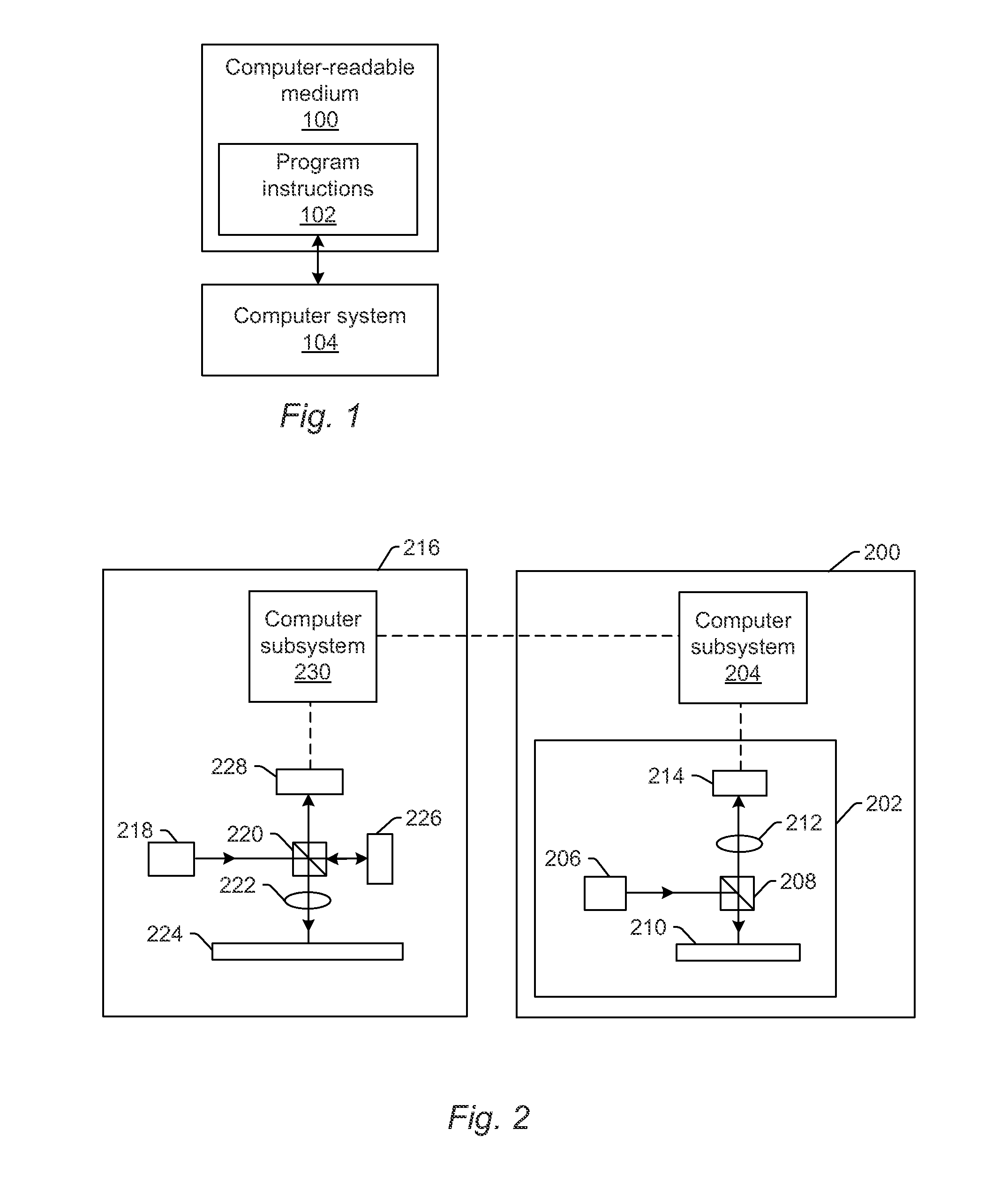
[0020]Turning now to the drawings, it is noted that the figures are not drawn to scale. In particular, the scale of some of the elements of the figures is greatly exaggerated to emphasize characteristics of the elements. It is also noted that the figures are not drawn to the same scale. Elements shown in more than one figure that may be similarly configured have been indicated using the same reference numerals. Unless otherwise noted herein, any of the elements described and shown may include any suitable commercially available elements.

[0021]One embodiment relates to a computer-implemented method for determining one or more parameters of a wafer inspection process. The method includes acquiring metrology data for a wafer generated by a wafer metrology system. Acquiring the metrology data may include performing measurements on the wafer such as any of those described further herein using a wafer metrology tool, which may be configured as described herein. In this manner, acquiring t...


PUM


Abstract

Methods and systems for determining one or more parameters of a wafer inspection process are provided. One method includes acquiring metrology data for a wafer generated by a wafer metrology system. The method also includes determining one or more parameters of a wafer inspection process for the wafer or another wafer based on the metrology data.

Description

BACKGROUND OF THE INVENTION[0001]1. Field of the Invention[0002]This invention generally relates to methods and systems for metrology optimized inspection in which metrology data for a wafer is used to alter one or more parameters of a wafer inspection process for the wafer or another wafer.[0003]2. Description of the Related Art[0004]The following description and examples are not admitted to be prior art by virtue of their inclusion in this section.[0005]Fabricating semiconductor devices such as logic and memory devices typically includes processing a substrate such as a semiconductor wafer using a large number of semiconductor fabrication processes to form various features and multiple levels of the semiconductor devices. For example, lithography is a semiconductor fabrication process that involves transferring a pattern from a reticle to a resist arranged on a semiconductor wafer. Additional examples of semiconductor fabrication processes include, but are not limited to, chemical...

Claims


Application Information

Patent Timeline
IPC IPC(8): G01N21/93G01N21/95
CPCG01N21/93G01N21/9501G01N2201/125G01N2201/105G01N2201/11G01N2201/061G01B11/0675G01N21/956G03F7/705G01B2210/56G03F7/70616G01B11/06
Inventor PARK, ALLENMACNAUGHTON, CRAIGCHANG, ELLIS
Owner KLA TENCOR CORP
Why Eureka
Try Eureka