Semiconductor device

a technology of semiconductor devices and semiconductors, applied in semiconductor devices, diodes, electrical apparatus, etc., can solve the problems of limiting the improvement of deterioration of other two, and inability to improve the performance of power semiconductor devices, so as to improve the tolerance against breakdown, prevent the destruction of semiconductor devices, and high response speed

Inactive Publication Date: 2015-06-04
NAT INST OF ADVANCED IND SCI & TECH
View PDF9 Cites 17 Cited by
  • Summary
  • Abstract
  • Description
  • Claims
  • Application Information

AI Technical Summary

Benefits of technology

[0080]According to the present invention, it is possible to realize a semiconductor device having an improved tolerance against breakdown, by providing a punch-through breakdown function in the semiconductor device. When a surge voltage drops, a semiconductor device in which a punch-through function is provided can let a punch-through breakdown occur at a high response speed and uniformly throughout the device. As a result, the semiconductor device can be prevented from destruction.
[0081]Here, a punch-through breakdown is a phenomenon in a semiconductor structure in which two semiconductor regions having a first conductivity type are PN junction-isolated from each other by means of at least one or more semiconductor region formed between the two semiconductor regions and having a second conductivity type, and ohmic electrodes are formed over the two semiconductor regions having the first conductivity type, respectively. When a positive or negative voltage is applied between the two ohmic electrodes, the semiconductor region having the second conductivity type is partially or wholly depleted to get the two semiconductor regions having the first conductivity type connected with each other through the depletion layer, which causes a current to flow between the two electrodes. This is the punch-through breakdown.
[0082]With the feature of (2) described above, it is possible to prevent destruction due to an avalanche breakdown and to thereby realize a highly reliable semiconductor device.
[0083]With the feature of (3) described above, a unipolar semiconductor device having a punch-through breakdown function can realize a behavior as a unipolar device including a breakdown state. Hence, when a surge voltage drops, the semiconductor device can let a punch-through breakdown occur at a high response speed and uniformly throughout the device.
[0084]With the feature of (4) described above, it is possible to solve the problem of avalanche breakdown in a semiconductor device made of a wide band gap semiconductor. Further, when a surge voltage drops, the semiconductor device can let a punch-through breakdown occur at a high response speed and uniformly throughout the device.
[0085]With the feature of (5) described above, a breakdown current flows by passing through a heterojunction interface having polarized charges having the same polarity as that of the carriers carrying the breakdown current. This makes it possible to prevent variation of a punch-through breakdown voltage due to temperature variation, and to realize a highly reliable semiconductor device in a broad temperature range. Here, the polarity of a carrier is negative for an electron, and positive for a hole. That is, when the carriers carrying a breakdown current are electrons, the breakdown current flow by passing through a hetero-interface having negatively polarized charges. When the carriers carrying a breakdown current are holes, the breakdown current flows by passing through a hetero-interface having positively polarized charges.

Problems solved by technology

However, in recent years, it has been pointed out that the performance of Si power semiconductor devices can no longer be improved because of the material properties of Si.
However, there is a trade-off relationship among these three properties, and when one is improved, the other two tend to deteriorate.
This is the cause of the limitation in the improvement of the performance of power semiconductor devices using Si.
However, wide band gap semiconductor devices when used as power converters have a problem that the devices may be destroyed by a surge voltage.
In this case, an avalanche breakdown occurs in the semiconductor device, and the device is destroyed if the breakdown state continues.
After this, the Vds is raised, and when the Vds reaches a predetermined voltage Vava, an avalanche breakdown occurs, and the drain current increases sharply.
Here, a device withstand voltage is a voltage at which a current that has started to flow during an Off state makes it no more possible for the Off state to be maintained.
When a surge voltage above the device withstand voltage occurs, a breakdown state occurs.
Therefore, it has a high did / dt value, and as a result, a surge voltage in the device is inherently high.
Further, since the device capacitance is small, a surge voltage that occurs due to energy accumulated in the floating inductance is high, even if the accumulated energy is low.
This is an unavoidable problem of a wide band gap semiconductor device that can be switched at a high speed.
As a second factor, a device is destroyed due to local concentration of an avalanche breakdown current in the device.
In a wide band gap semiconductor device, an avalanche breakdown cannot occur uniformly throughout the device, and the breakdown current tends to concentrate.
This problem is attributed to the fact that a P type and an N type of a wide band gap semiconductor cannot have low resistivities at the same time.
Therefore, electrons and holes from inside the device, which are generated by avalanche multiplication, cannot be eliminated efficiently.
As a result, a breakdown current concentrates at the location at which an avalanche breakdown started, and the device is destroyed at the location of the concentration.
Hence, when a strong electric field that would cause an avalanche breakdown is applied, a dielectric breakdown occurs in the protective insulation film not in the semiconductor.
As a result, the breakdown current concentrates at the predetermined location in the device, leading to a local destruction.
The current concentration in the device during a behavior as a bipolar device causes device destruction.
Due to the second factor, wide band gap semiconductor devices characterized in that the carriers carrying an On current during an On state are electrons have particularly outstanding avalanche breakdown destruction.
In this case, it does not include a P-type region and an electrode for the P-type region through which holes generated by an avalanche are eliminated, which makes it harder for the holes to be eliminated.
As a result, holes generated by avalanche multiplication are accumulated in the device.
Hence, the device is destroyed even by a weak avalanche current.
However, the fundamental problem of an avalanche breakdown in a wide band gap semiconductor described above is not resolved.
However, destruction of a wide band gap semiconductor device due to an avalanche breakdown is a problem shared in common among various wide band gap semiconductor devices, which is attributed to a high surge voltage, a uniform avalanche breakdown in the whole device, and deterioration of an insulation film by a strong electric filed that would cause an avalanche breakdown, as described above.
Specifically, unipolar and bipolar devices have the same problem.
More specifically, wide band gap devices described below have the same problem.
For a first reason, a lateral semiconductor device has a switching speed higher than that of a vertical semiconductor device, and incurs a high surge voltage as a result.
For a second reason, high energy carriers generated by an avalanche breakdown flow through the surface of the semiconductor device and are injected into an insulation film protecting the surface of the semiconductor device, to thereby cause concentration of an electric field in the insulation film, leading to a destruction in the insulation film.

Method used


Image

  • Semiconductor device
  • Semiconductor device
  • Semiconductor device

Examples


example 1

First Embodiment

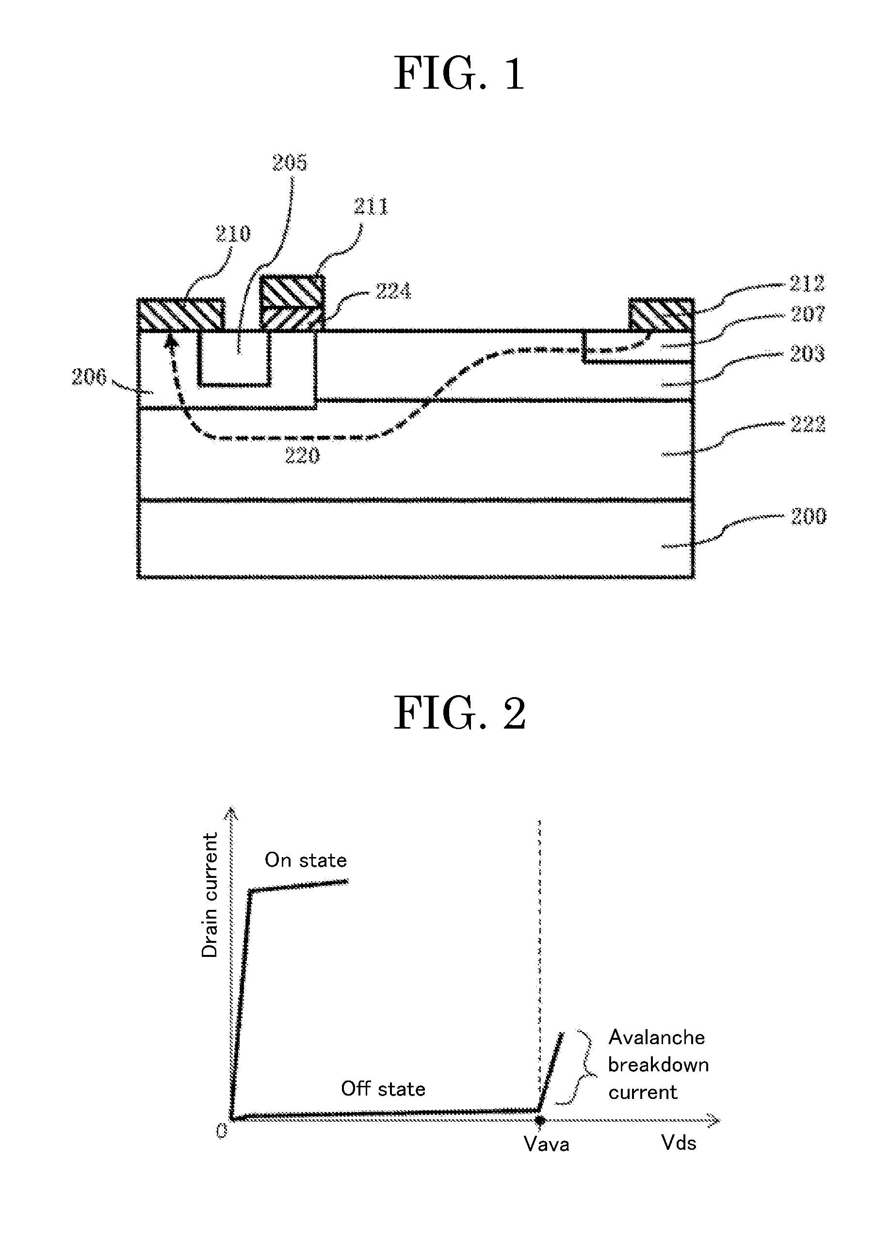
[0141]A HFET made of a nitride semiconductor, which is the first embodiment, will be explained. FIG. 4 shows a configuration diagram of a nitride semiconductor HFET according to the present invention. The semiconductor material of the HFET except for a substrate 100 is a nitride semiconductor having a chemical formula represented by the following formula (3).

BxAlyInzGa1-x-y-zN  (3)

[0142]In the formula, x, y, and z have values that satisfy 0≦x≦1, 0≦y≦1, 0≦z≦1, and x+y≦z≦1. The material of the substrate 100 needs not be a nitride semiconductor.

[0143]It is preferable that the layer structure of the present invention be formed in a c-axis direction of a hexagonal crystal structure. The c-axis direction is a [0001] or [000-1] direction.

[0144]It is preferable that the material of the substrate 100 be a material over which a high-quality crystal growth of a nitride semiconductor can be realized. Examples of the material include a Si substrate, a SOI (Silicon-on-Insulator) s...

example 2

Second Embodiment

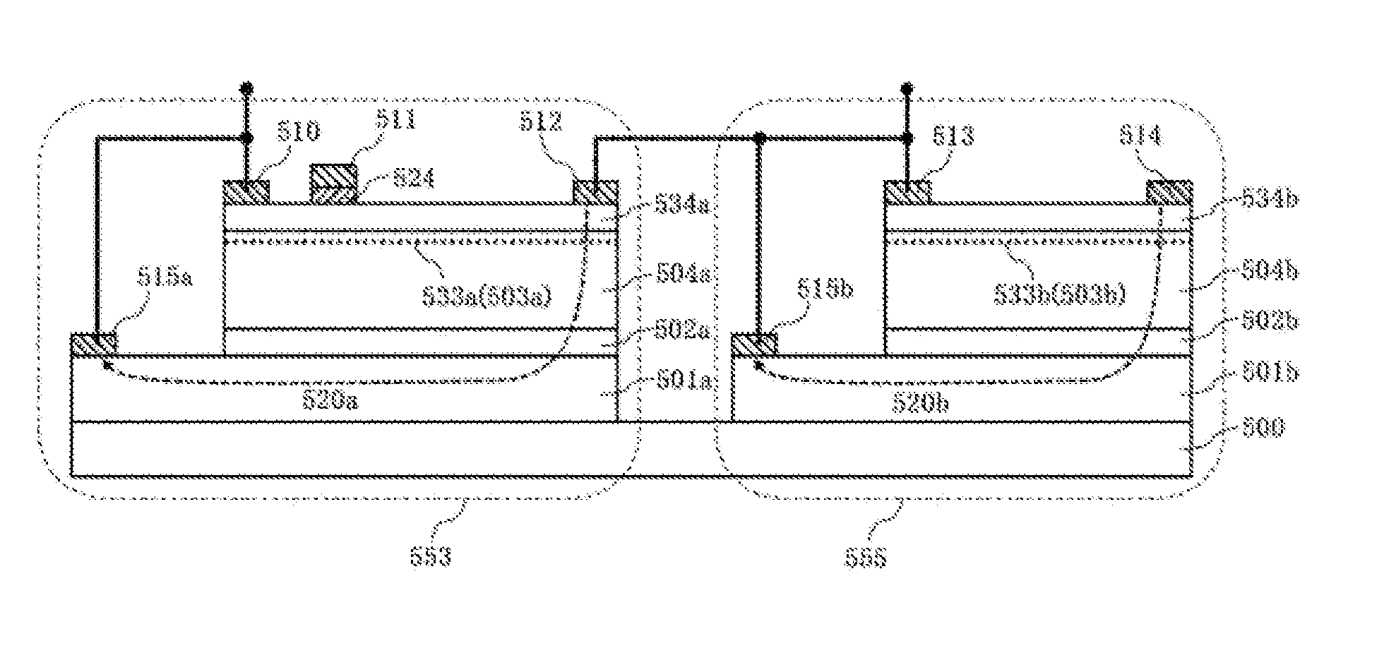
[0220]A MISFET made of SiC, which is the second embodiment, will be explained. FIG. 37 shows a structure diagram of a MISFET made of SiC according to the present invention. The semiconductor material forming the MISFET is SiC, except for a substrate 200. It is preferable that the polytype of SiC be 3C, 6H, and 4H. The substrate 200 may be made of a material other than SiC.

[0221]Further, a polytype is particularly preferably 6H and 4H of a hexagonal crystal system, and it is preferable that the layer structure be formed in a c-axis direction of a hexagonal crystal structure. The c-axis direction is a [0001] or [000-1] direction. A dielectric constant in the c-axis direction is higher than the dielectric constant in the a-axis direction. Therefore, the trade-off among a punch-through breakdown voltage, an avalanche breakdown voltage, and a characteristic On resistance can be resolved, and a high device withstand voltage and an On resistance can be achieved simultaneou...

example 3

Third Embodiment

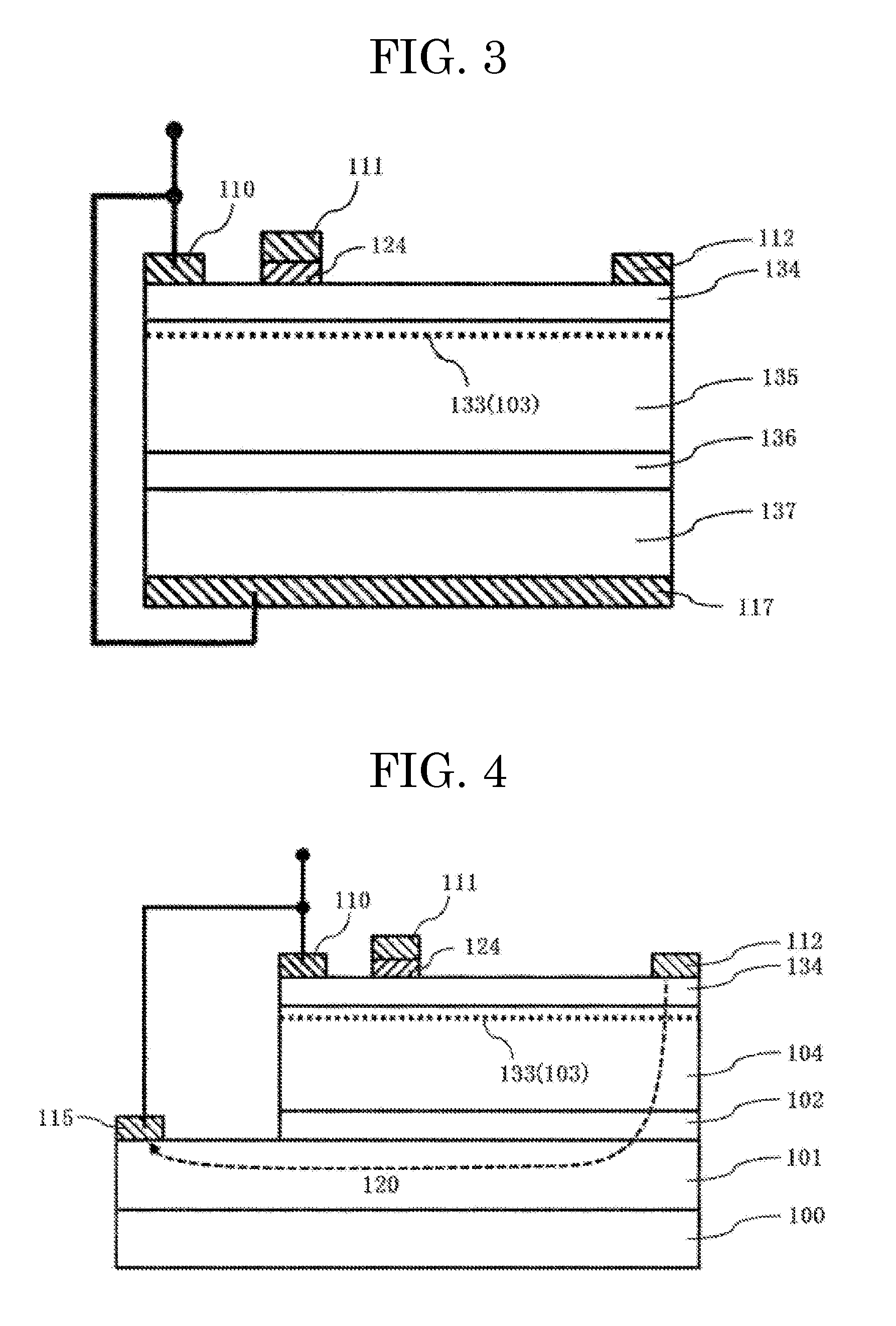
[0247]A JFET made of SiC, which is the third embodiment, will be explained. FIG. 40 shows a configuration diagram of a MISFET made of SiC according to the present invention. The semiconductor material forming the MISFET is SiC, except for a substrate 300. It is preferable that the polytype of SiC be 3C, 6H, and 4H. The substrate 300 may be made of a material other than SiC.

[0248]Further, a polytype is particularly preferably 6H and 4H of a hexagonal crystal system, and it is preferable that the layer structure be formed in a c-axis direction of a hexagonal crystal structure. The c-axis direction is a [0001] or [000-1] direction. A dielectric constant in the c-axis direction is higher than the dielectric constant in the a-axis direction. Therefore, the trade-off among a punch-through breakdown voltage, an avalanche breakdown voltage, and a characteristic On resistance can be resolved, and a high device withstand voltage and an On resistance can be achieved simultaneou...


PUM


Abstract

The present invention provides a semiconductor device that prevents destruction due to an avalanche breakdown and that has a high tolerance against breakdown by configuring the device so as to have a punch-through breakdown function therein and such that the breakdown voltage of a punch-through breakdown is lower than an avalanche breakdown voltage so that an avalanche breakdown does not occur.

Description

TECHNICAL FIELD[0001]The present invention relates to a semiconductor device, and particularly to a power semiconductor device having an improved tolerance against breakdown.BACKGROUND ART[0002]Power semiconductor devices are mainly used for power converters (DC-DC, AC-DC, DC-AC, and DC-DC), and high-frequency power amplifiers. Up until now, Si power semiconductor devices have been used widely. However, in recent years, it has been pointed out that the performance of Si power semiconductor devices can no longer be improved because of the material properties of Si.[0003]Among properties required of power semiconductor devices, important are three properties, namely a high device withstand voltage, a low On resistance, and a low device capacitance. However, there is a trade-off relationship among these three properties, and when one is improved, the other two tend to deteriorate. This is the cause of the limitation in the improvement of the performance of power semiconductor devices u...

Claims


Application Information

Patent Timeline
Patent Type & Authority Applications(United States)
IPC IPC(8): H01L27/02H01L29/04H01L29/78H01L29/16H01L29/872
CPCH01L27/0266H01L29/1608H01L29/872H01L27/0255H01L29/04H01L29/045H01L29/7841H01L29/7816H01L27/0605H01L27/0629H01L29/1075H01L29/1083H01L29/1087H01L29/41725H01L29/7787H01L29/7835H01L29/8083H01L29/4236H01L29/475H01L29/1066H01L29/1602H01L29/205H01L29/2003H01L27/0248H01L21/0455H01L21/049H01L29/1029H01L29/66068
Inventor NAKAJIMA, AKIRANISHIZAWA, SHINICHIOHASHI, HIROMICHI
Owner NAT INST OF ADVANCED IND SCI & TECH
Why Eureka
Try Eureka