System and method of storing data at a non-volatile memory

Inactive Publication Date: 2015-06-18
SANDISK TECH LLC
View PDF9 Cites 17 Cited by
  • Summary
  • Abstract
  • Description
  • Claims
  • Application Information

AI Technical Summary

Benefits of technology

[0009]To account for uneven wear among the dies of the non-volatile memory resulting from the at least one die used in the single-bit mode, the at least one die determined (e.g., selected) to be used in the single-bit mode may be shuffled (e.g., rotated) across the dies (e.g., over time) and need not be restricted to one die at all times. Using the mixed mode programming scheme in the data storage device may result in a cost savings and a power savings as compared to data storage devices that stripe data across multiple dies using a single programming scheme, such as a single-bit programming mode or a multi-bit programming mode. Additionally, a certain amount of die overprovisioning may be required to meet a target total storage capacity. In a first approach, the data storage device may overprovision dies (e.g., include a total number of dies that is greater than a number of dies that can be programmed concurrently) to meet the target total storage capacity. In a second approach, the data storage device may include a total number of dies that is equal to a number of dies that can be programmed concurrently. Accordingly, in the second approach, a total storage capacity may be less than the target total storage capacity. The second approach may result in a total storage capacity that is less than the t

Problems solved by technology

However, if the achievable data storage rate (N*P) using the MLC dies would not meet the product performance, such as the data storage rate, the data storage device may be designed using Single-Level Cell (SLC) dies.
Having to use twice the number of dies (e.g., a number of SLC dies as compared to a number of MLC dies) to satisfy a data storage rate requirement results in additional monetary costs when designing and producing the data storage device and results in additional power consumption when operating the data storage device.
The second approach may result in a total storage capacity that is le

Method used


Image

  • System and method of storing data at a non-volatile memory
  • System and method of storing data at a non-volatile memory
  • System and method of storing data at a non-volatile memory

Examples


Example

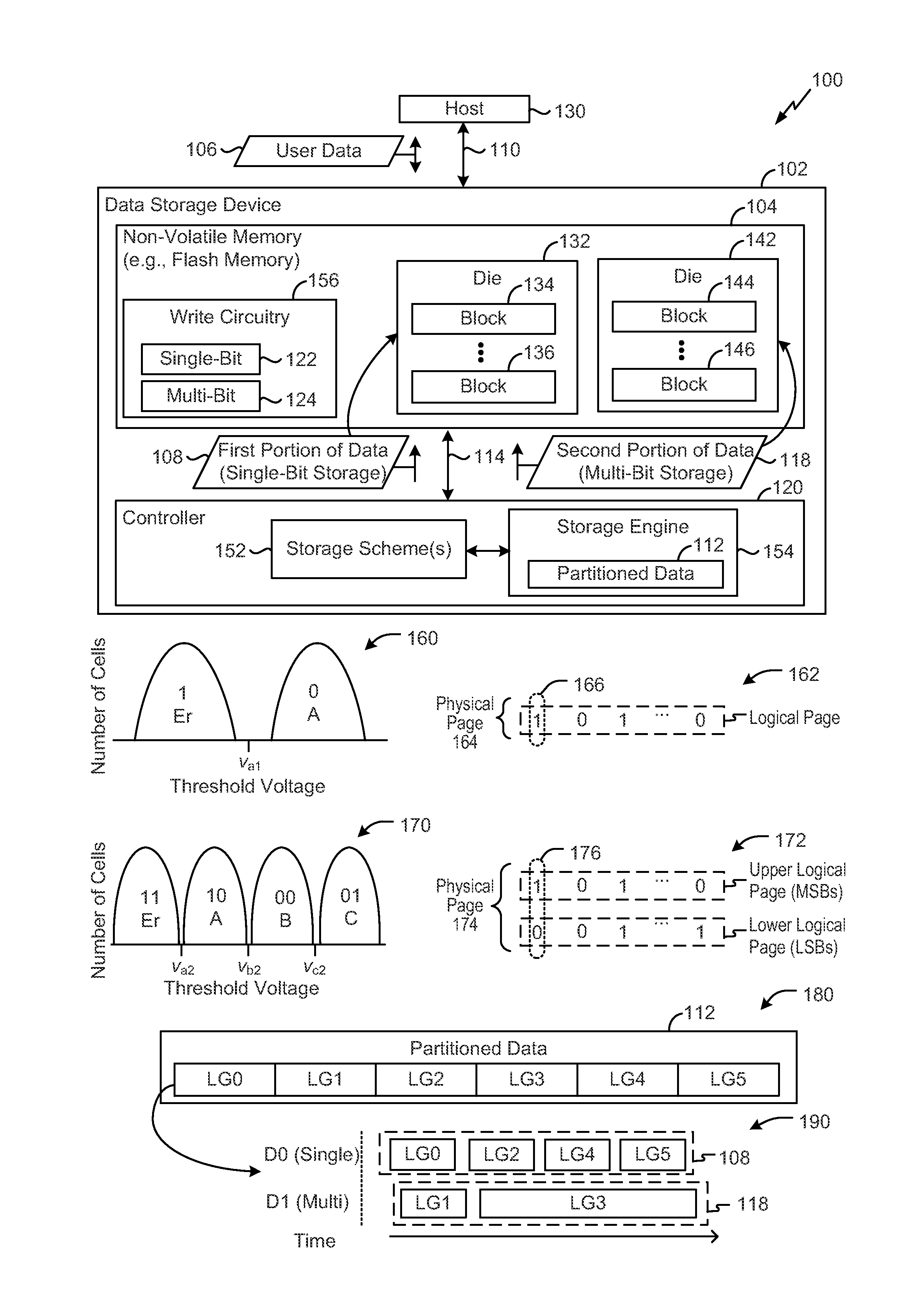
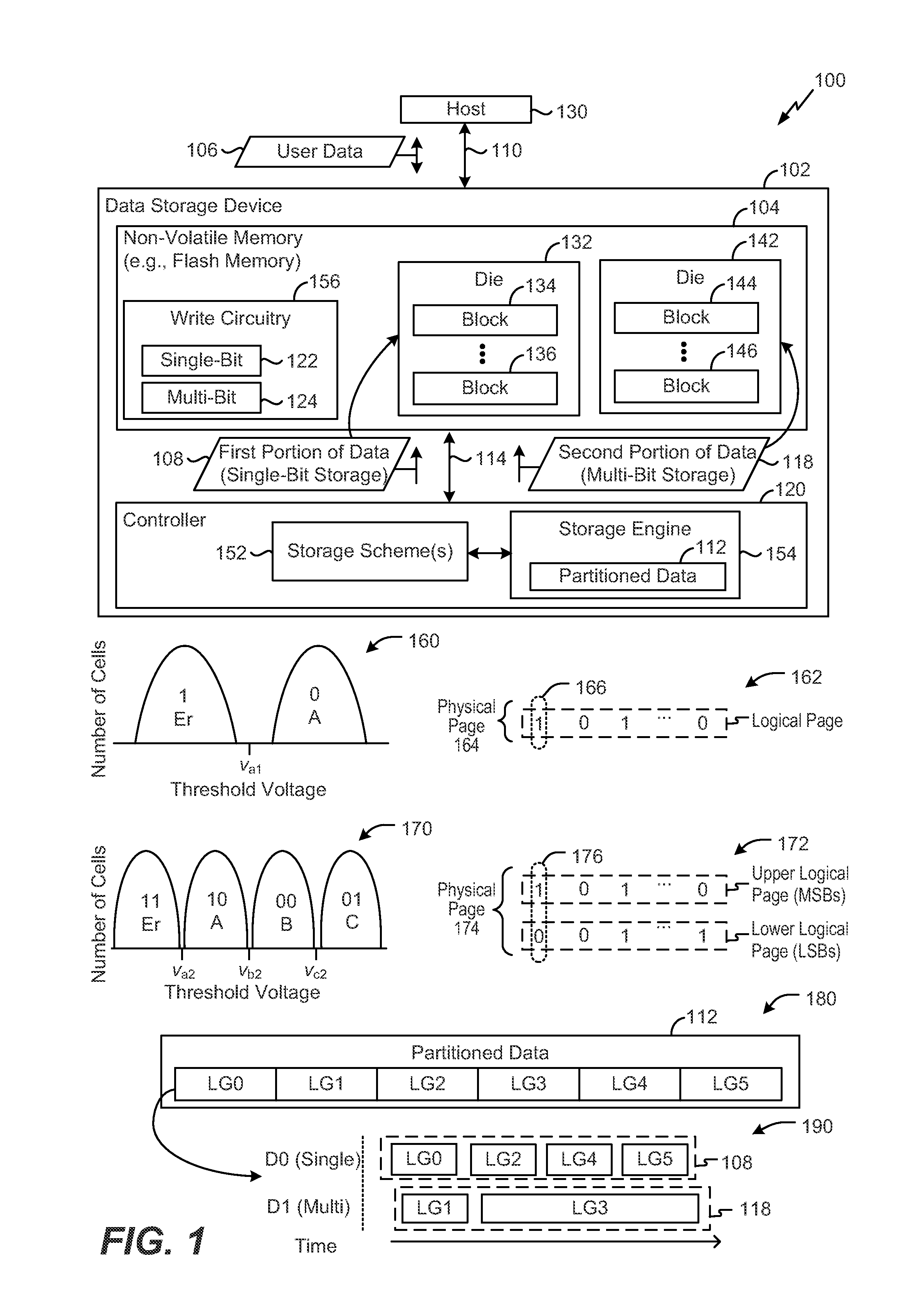
[0021]Particular embodiments of the present disclosure are described below with reference to the drawings. In the description, common features are designated by common reference numbers throughout the drawings.

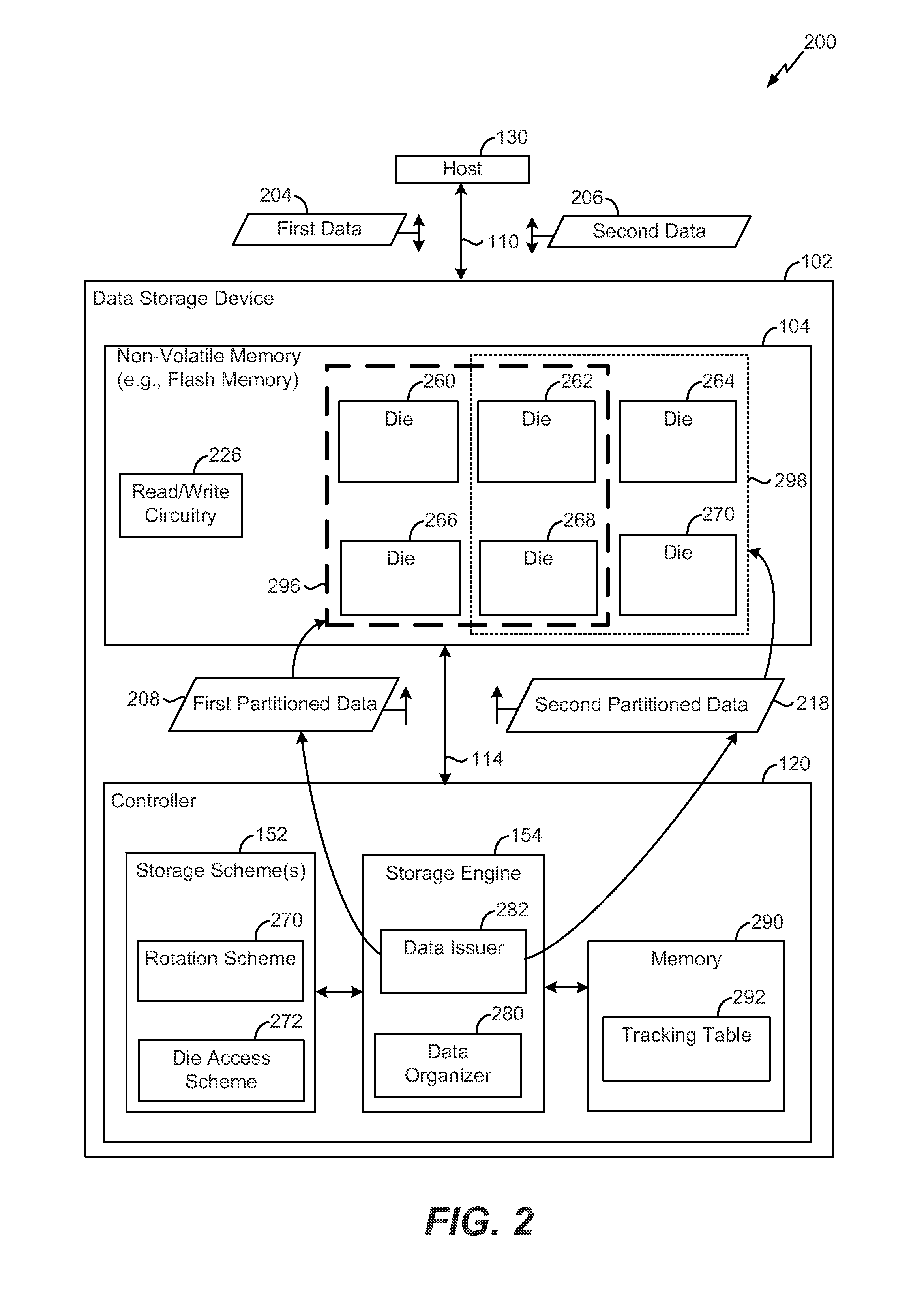
[0022]FIG. 1 is a block diagram of a particular illustrative embodiment of an electronic device 100 including a data storage device 102 and a host device 130. The data storage device 102 may be coupled to the host device 130 via a communication path 110, such as a wired communication path and / or a wireless communication path. The data storage device 102 may be embedded within the host device 130, such as in accordance with an embedded MultiMedia Card (eMMC®) (trademark of Joint Electron Devices Engineering Council (JEDEC) Solid State Technology Association, Arlington, Va.) configuration. Alternatively, the data storage device 102 may be removable from (i.e., “removably” coupled to) the host device 130. For example, the data storage device 102 may be removably coupled to the ho...


PUM


Abstract

A data storage device includes a controller coupled to a non-volatile memory that includes a plurality of dies. The plurality of dies includes a first die and a second die. The controller is configured to receive data to be stored into the non-volatile memory and to partition the data into a first portion and a second portion. The controller is further configured to store the first portion into the first die and to store the second portion into the second die. The first portion is stored into the first die using a single-bit mode. The second portion is stored into the second die using a multi-bit mode.

Description

CROSS-REFERENCE TO RELATED APPLICATIONS[0001]The present application claims priority from Indian Application No. 5726 / CHE / 2013, filed Dec. 12, 2013, the contents of which are incorporated by reference herein in their entirety.FIELD OF THE DISCLOSURE[0002]The present disclosure is generally related to storing data at a non-volatile memory.BACKGROUND[0003]Non-volatile data storage devices, such as embedded memory devices (e.g., embedded MultiMedia Card (eMMC) devices) and removable memory devices (e.g., removable universal serial bus (USB) flash memory devices and other removable storage cards), have allowed for increased portability of data and software applications. Users of non-volatile data storage devices increasingly rely on the non-volatile storage devices to store and provide rapid access to a large amount of data. For example, a user may store large audio files, images, videos, and other files at a data storage device.[0004]A data storage device including a non-volatile memor...

Claims


Application Information

Patent Timeline
IPC IPC(8): G06F3/06
CPCG06F3/0608G06F2206/1014G06F3/0644G06F3/0679G06F3/0625G06F3/0659G06F3/0688Y02D10/00
Inventor SIVASANKARAN, VIJAYMANOHAR, ABHIJEETNAGABHIRAVA, RAJEEVMURALIDHARAN, KIRAN KUMAR
Owner SANDISK TECH LLC
Why Eureka
Try Eureka