High throughput scanning probe microscopy device

Active Publication Date: 2015-07-02
NEDERLANDSE ORG VOOR TOEGEPAST-NATUURWETENSCHAPPELIJK ONDERZOEK (TNO)
View PDF1 Cites 4 Cited by
  • Summary
  • Abstract
  • Description
  • Claims
  • Application Information

AI Technical Summary

Benefits of technology

The present invention aims to solve problems in the prior art by providing a scanning probe microscopy device that can quickly and efficiently scan multiple sites on a surface.

Problems solved by technology

The very high resolution and accuracy of this technology however comes at the cost of performance in terms of throughput.
As will be appreciated, this process may be rather slow.
Even though the above has lead to an improvement in throughput, the scanning of multiple sites on a sample surface still takes a considerable amount of time.
For this and other reasons, application of this technique in industrial environments, for example for the testing of wafers in semiconductor industry, is far from ideal.

Method used


Image

  • High throughput scanning probe microscopy device
  • High throughput scanning probe microscopy device
  • High throughput scanning probe microscopy device

Examples


Embodiment Construction

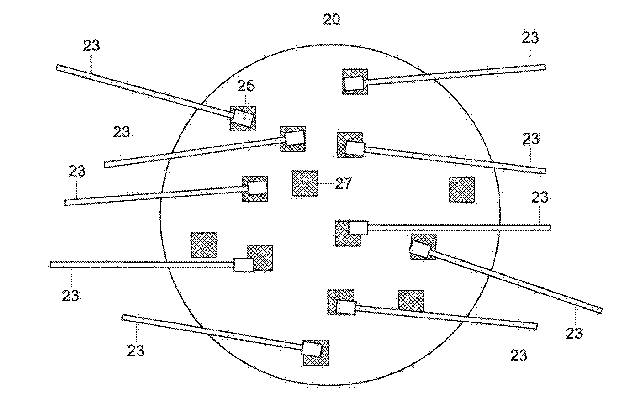
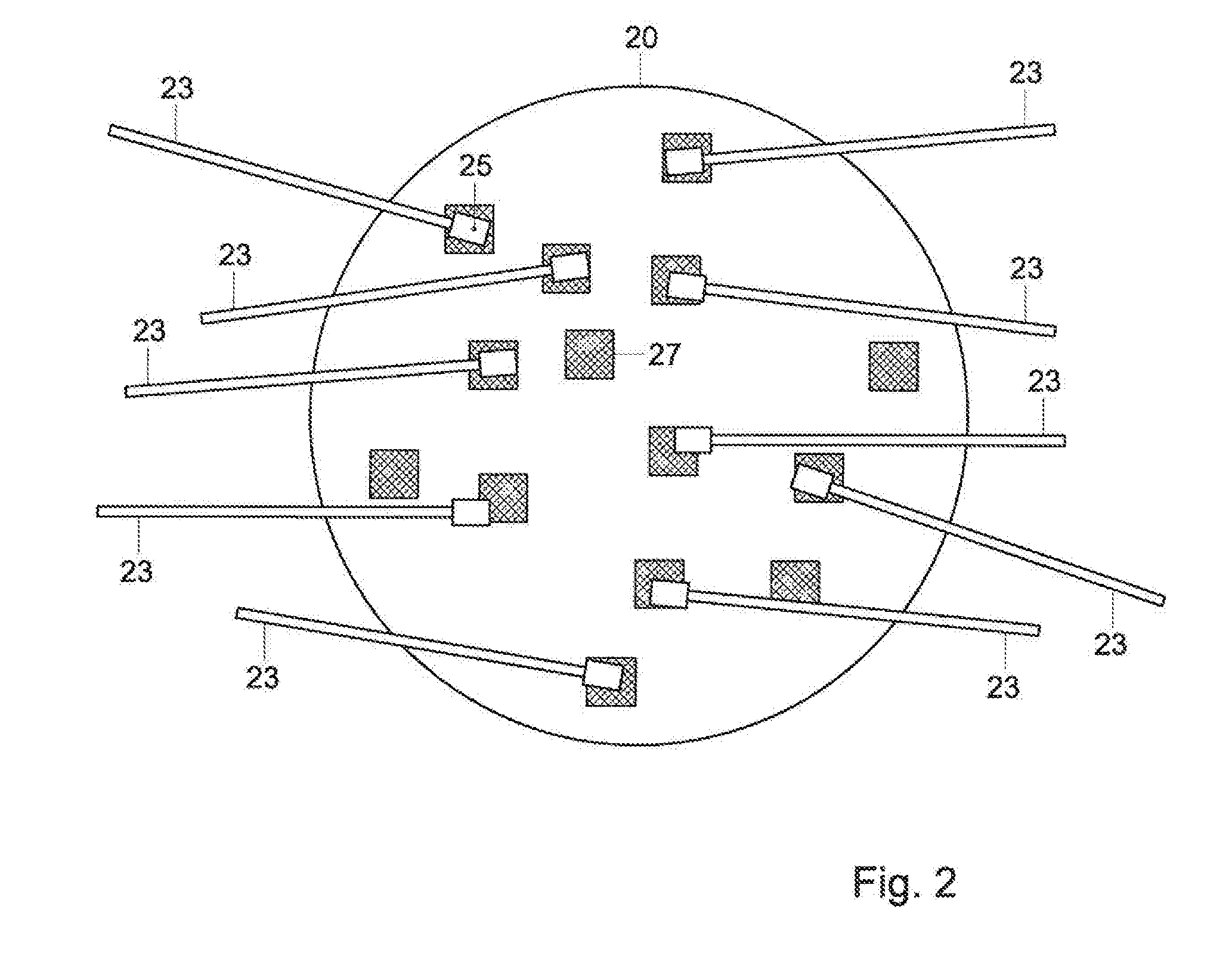
[0029]The scanning probe microscopy device of the present invention may for example be an atomic force microscopy (AFM) device. Although in the description below reference will be made to particularly the embodiment of an atomic force microscopy device, the teachings of this document are not restricted to such an application. As will be appreciated the teachings of the invention may be applied to any microscopy device that is based on the principles of scanning a surface region using a probe. Particular fields of applications have been mentioned earlier in this document.

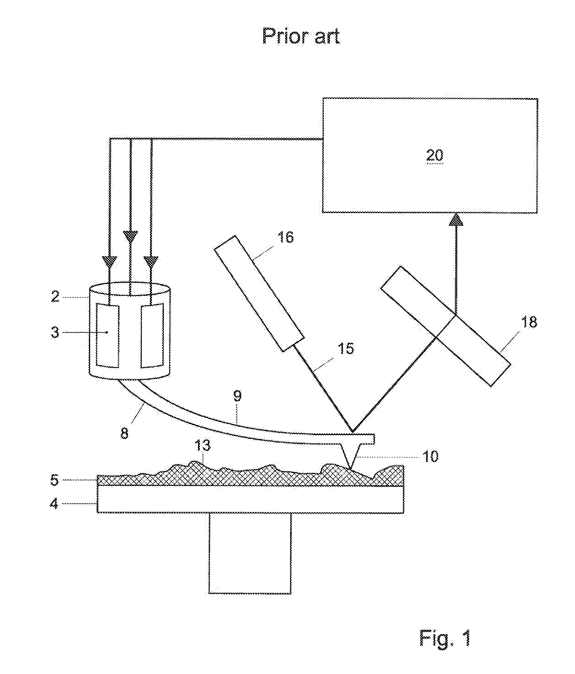
[0030]FIG. 1 schematically illustrates the working principle of a typical prior art atomic force microscope. In FIG. 1, a probe head 2 comprises piezo type drivers 3 for the X-, Y-, and Z-directional motion of a probe 8. The probe 8 consists of a cantilever 9 having a probe tip 10 arranged for scanning a sample surface 5. During scanning, a dither piezo (not shown) may drive the cantilever in vibrational mode, for ex...


PUM


Abstract

A scanning probe microscopy device for mapping nanostructures on a sample surface of a sample is provided. The device may comprise a plurality probes for scanning the sample surface, and one or more motion actuators for enabling motion of the probes relative to the sample, wherein each of the plurality of probes comprises a probing tip mounted on a cantilever arranged for bringing the probing tip in contact with the sampling surface for enabling the scanning. The device may further comprise a plurality of Z-position detectors for determining a position of each probing tip along a Z-direction when the probing tip is in contact with the sample surface, wherein the Z-direction is a direction transverse to the sample surface, for enabling mapping of the nanostructures.

Description

FIELD OF THE INVENTION[0001]The present invention is directed to an scanning probe microscopy device for mapping nanostructures on a sample surface of a sample, comprising a plurality probes for scanning the sample surface, and one or more motion actuators for enabling motion of the probes relative to the sample, wherein each of said plurality of probes comprises a probing tip mounted on a cantilever arranged for bringing the probing tip in contact with the sampling surface for enabling the scanning, the device further comprising a plurality of Z-position detectors for determining a position of each probing tip along a Z-direction when the probing tip is in contact with the sample surface, wherein the Z-direction is a direction transverse to the sample surface, for enabling mapping of the nanostructures.BACKGROUND[0002]Scanning probe microscopy (SPM) devices, such as atomic force microscopy (AFM) devices as described above are for example applied in the semiconductor industry for sc...

Claims


Application Information

Patent Timeline
IPC IPC(8): G01Q10/04
CPCG01Q10/04G01Q60/38G01Q70/06B82Y35/00
Inventor SADEGHIAN MARNANI, HAMEDVAN DEN DOOL, TEUNIS CORNELISRIJNVELD, NIEK
Owner NEDERLANDSE ORG VOOR TOEGEPAST-NATUURWETENSCHAPPELIJK ONDERZOEK (TNO)
Why Eureka
Try Eureka