Power semiconductor module

a technology of semiconductor modules and semiconductor components, applied in semiconductor devices, semiconductor/solid-state device details, cooling/ventilation/heating modifications, etc., can solve the problems of increasing package cost, reducing productivity, and increasing the cost of the package process

Active Publication Date: 2015-07-30
SAMSUNG ELECTRO MECHANICS CO LTD
View PDF1 Cites 3 Cited by
  • Summary
  • Abstract
  • Description
  • Claims
  • Application Information

AI Technical Summary

Benefits of technology

[0029]The first terminal may be provided with a gate window to prevent interference due t

Problems solved by technology

In the power semiconductor module, a high-capacity power semiconductor module uses a plurality of power devices which are connected to each other in parallel, due to a limitation of the power device.
The high-capacity power semiconductor module according to the related art, including the (Patent Document 1) has a problem in that there is a need to uniformly control each power device and the power devices are disposed only in a limited space and a limited number of power devices are connected to each other in parallel due to an unbalance of a heat generation problem between the power devices, and the like.
Therefore, to resolve the heat generation problem of the power device, in addition to a generally used heat radiating substrate, various efforts have been conducted, but do not obtain distinct outcomes.
Here, a structure of connecting between the terminals by the soldering has a problem of reliability of

Method used


Image

  • Power semiconductor module
  • Power semiconductor module
  • Power semiconductor module

Examples


first preferred embodiment

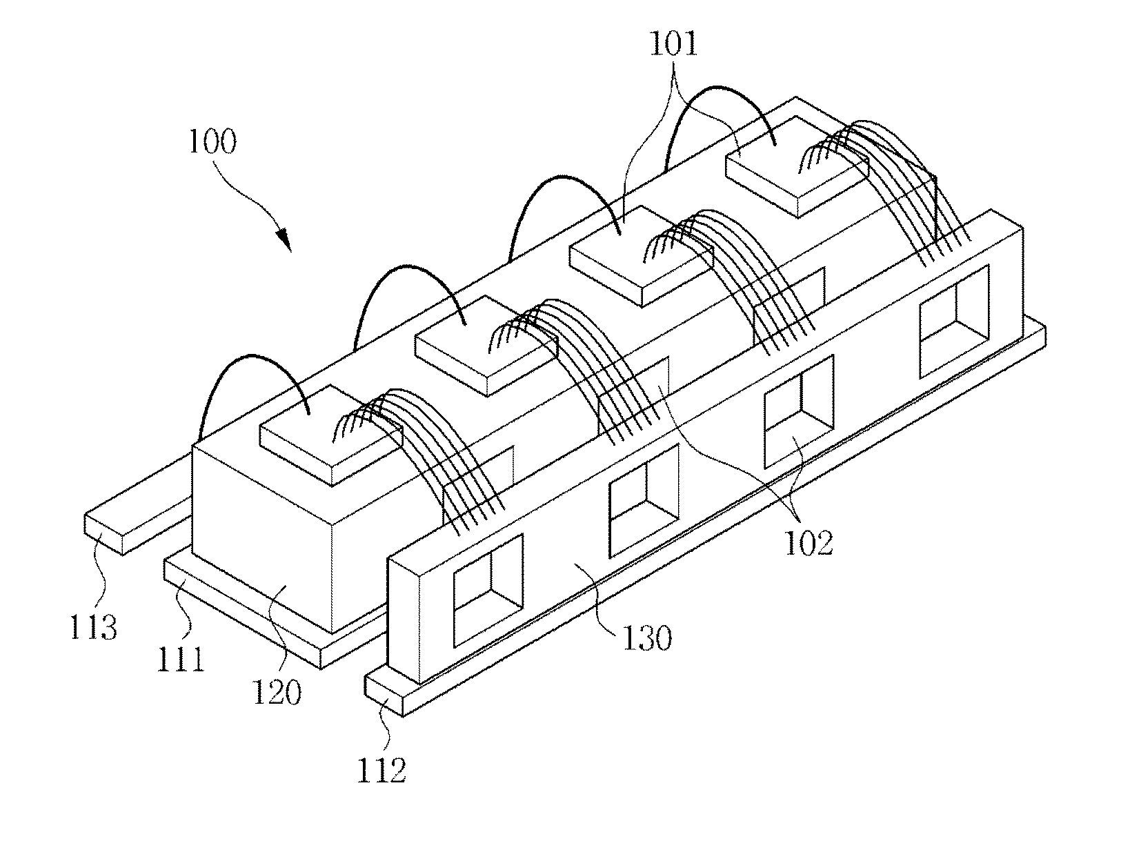
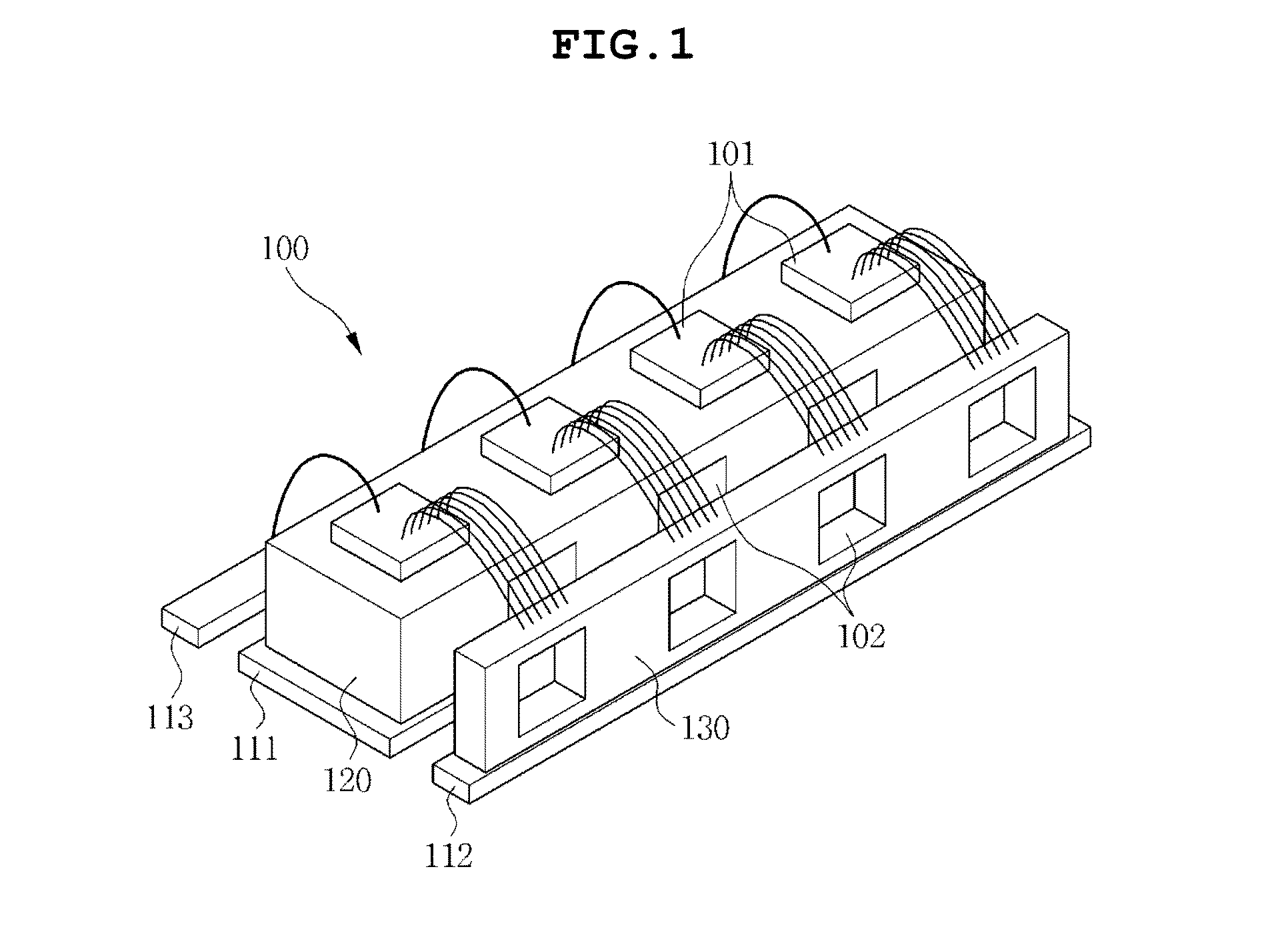
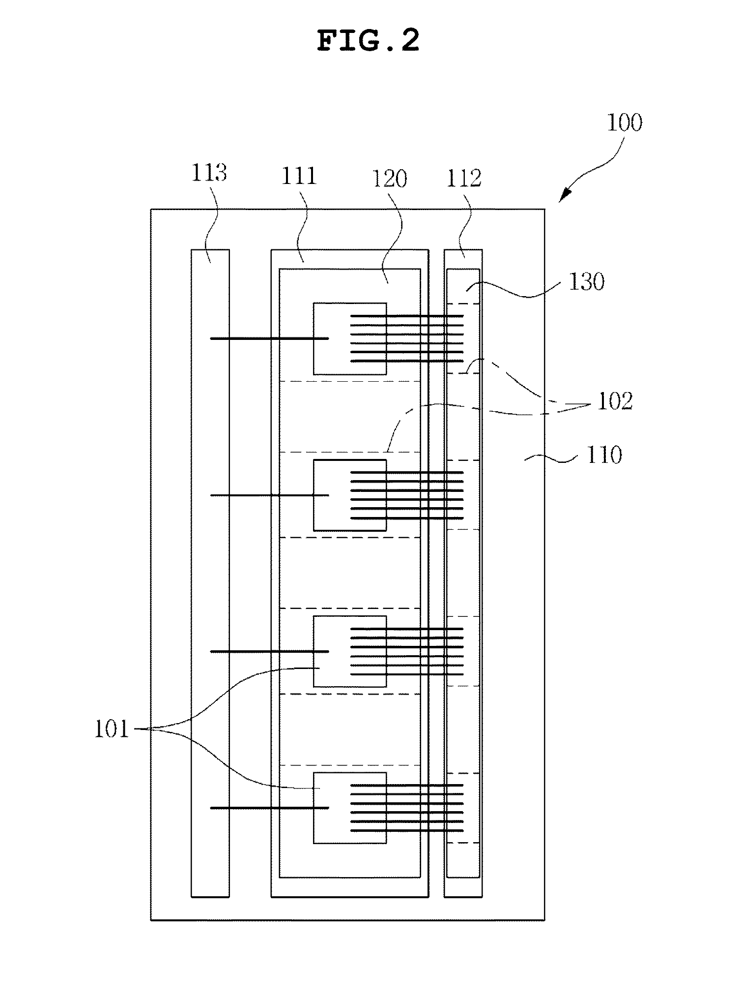
[0043]As illustrated in FIGS. 1 and 2, a power semiconductor module 100 according to a first preferred embodiment of the present invention has a structure in which four large-capacity power devices including MOSFET, IGBT, and FRD, and the like are connected to one another in parallel, in which a power device 101 is mounted on a heat spreader having three terminal slots disposed on a side thereof.

[0044]The power device 101 has a source part which is electrically connected to another heat spreader which is disposed on one side of the heat spreader and a gate signal terminal is electrically connected to a pattern on a printed circuit board (PCB). As an example of the electrical connection, wire bonding is used.

[0045]Here, it is to be noted that the heat spreader and another heat spreader may be divided into a first heat spreader 120 and a second heat spreader 130 to avoid confusion which is caused due to the same term. Further, the second heat spreader 130 has a side provided with four...

second preferred embodiment

[0052]As illustrated in FIG. 5, a power semiconductor module 200 according to a second preferred embodiment of the present invention has a structure in which four large-capacity power devices including MOSFET, IGBT, and FRD, and the like are connected to one another in parallel, in which a power device 201 is mounted on a heat spreader provided with three terminal slots.

[0053]The power device 201 has a source part which is electrically connected to another heat spreader which is disposed on one side of the heat spreader and a gate signal terminal is electrically connected to a pattern on the printed circuit board (PCB) which is disposed in an internal space 200b of a housing. As an example of the electrical connection, wire bonding is used.

[0054]Here, it is to be noted that the heat spreader and another heat spreader may be divided into a first heat spreader 220 and a second heat spreader 230 to avoid confusion which is caused due to the same term. Further, the second heat spreader ...

third preferred embodiment

[0061]As illustrated in FIG. 6, a power semiconductor module 300 according to a third preferred embodiment of the present invention has a structure in which four large-capacity power devices including MOSFET, IGBT, and FRD, and the like are mounted on a main heat spreader and are connected to one another in parallel. Further, the power semiconductor module 300 has a structure in which four large-capacity power devices 301 are mounted on another main heat spreader and are connected to one another in parallel.

[0062]In this configuration, the main heat spreader and the another main heat spreader are be divided into a first main heat spreader 320 and a second main heat spreader 321 to avoid confusion which is caused due to the same term, in which one surface of the first main spreader 320 and one surface of the second main heat spreader 321 are each provided with terminal slots 302.

[0063]The power device 301 of the first main heat spreader 320 has a source part which is electrically con...


PUM


Abstract

Disclosed herein is a power semiconductor module. The power semiconductor module includes: a printed circuit board (PCB); first and second heat spreaders mounted on the PCB and having one surface arranged with terminal slots; power devices mounted on the first heat spreader and connected to one another in parallel and electrically connected to the second heat spreader; and first and second terminals provided with protrusion inserted into the terminal slots and provided with connection terminals for connecting external terminals. Therefore, it is possible to improve heat radiating properties of the power semiconductor module and improve a reliability problem such as solder crack or delamination in connection with terminal connection.

Description

CROSS REFERENCE TO RELATED APPLICATION[0001]This application claims the benefit of Korean Patent Application No. 10-2014-0010455, filed on Jan. 28, 2014, entitled “Power Semiconductor Module” which is hereby incorporated by reference in its entirety into this application.BACKGROUND OF THE INVENTION[0002]1. Technical Field[0003]The present invention relates to a power semiconductor module.[0004]2. Description of the Related Art[0005]In the power semiconductor module, a high-capacity power semiconductor module uses a plurality of power devices which are connected to each other in parallel, due to a limitation of the power device. That is, according to the power semiconductor module published in (Patent Document 1), the high-capacity power semiconductor module is configured by mounting the plurality of power devices on a base plate and connecting the power devices in parallel to easily accommodate a high-capacity current.[0006]The high-capacity power semiconductor module according to t...

Claims


Application Information

Patent Timeline
IPC IPC(8): H01L23/34H01L23/00
CPCH01L24/49H01L23/34H01L2924/13055H01L24/48H01L2224/48091H01L2224/49111H01L2224/49113H01L2224/49175H01L2924/00014H01L2924/13091H01L25/072H01L2224/48227H01L2224/48229H01L2924/00H01L2224/45099H01L2224/05599
Inventor KIM, KWANG SOOCHAE, JOON SEOKHONG, CHANG SEOBKWAK, YOUNG HOONLEE, YOUNG KI
Owner SAMSUNG ELECTRO MECHANICS CO LTD
Why Eureka
Try Eureka