Lipseals and contact elements for semiconductor electroplating apparatuses

a technology of contact elements and electroplating apparatuses, which is applied in the direction of sealing devices, contact devices, manufacturing tools, etc., can solve the problems of more difficult to establish an optimal electrical connection with the substrate, and the potential corrosive properties of the electroplating solution

Active Publication Date: 2015-08-06
NOVELLUS SYSTEMS
View PDF5 Cites 27 Cited by
  • Summary
  • Abstract
  • Description
  • Claims
  • Application Information

AI Technical Summary

Problems solved by technology

However, in some configurations, a conductive seed layer on the substrate contacted by the electrical connections may become thinner towards the edge of the substrate, making it more difficult to establish an optimal electrical connection with the substrate.
Another issue arising in electroplating is the potentially corrosive properties of the electroplating solution.

Method used


Image

  • Lipseals and contact elements for semiconductor electroplating apparatuses
  • Lipseals and contact elements for semiconductor electroplating apparatuses
  • Lipseals and contact elements for semiconductor electroplating apparatuses

Examples


Embodiment Construction

[0036]In the following description, numerous specific details are set forth in order to provide a thorough understanding of the presented concepts. The presented concepts may be practiced without some or all of these specific details. In other instances, well known process operations have not been described in detail so as to not unnecessarily obscure the described concepts. While some concepts will be described in conjunction with specific embodiments, it will be understood that these embodiments are not intended to be limiting.

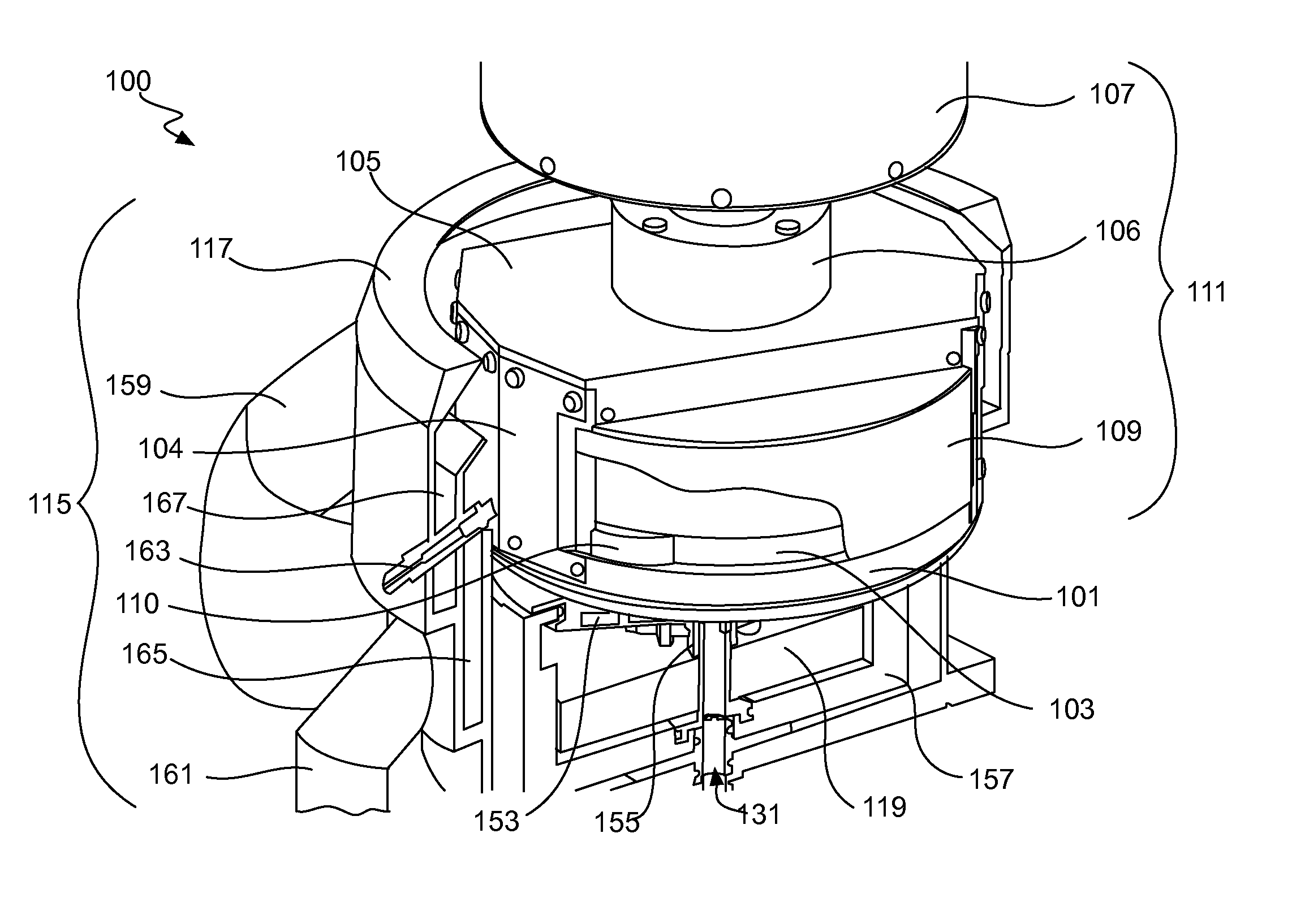
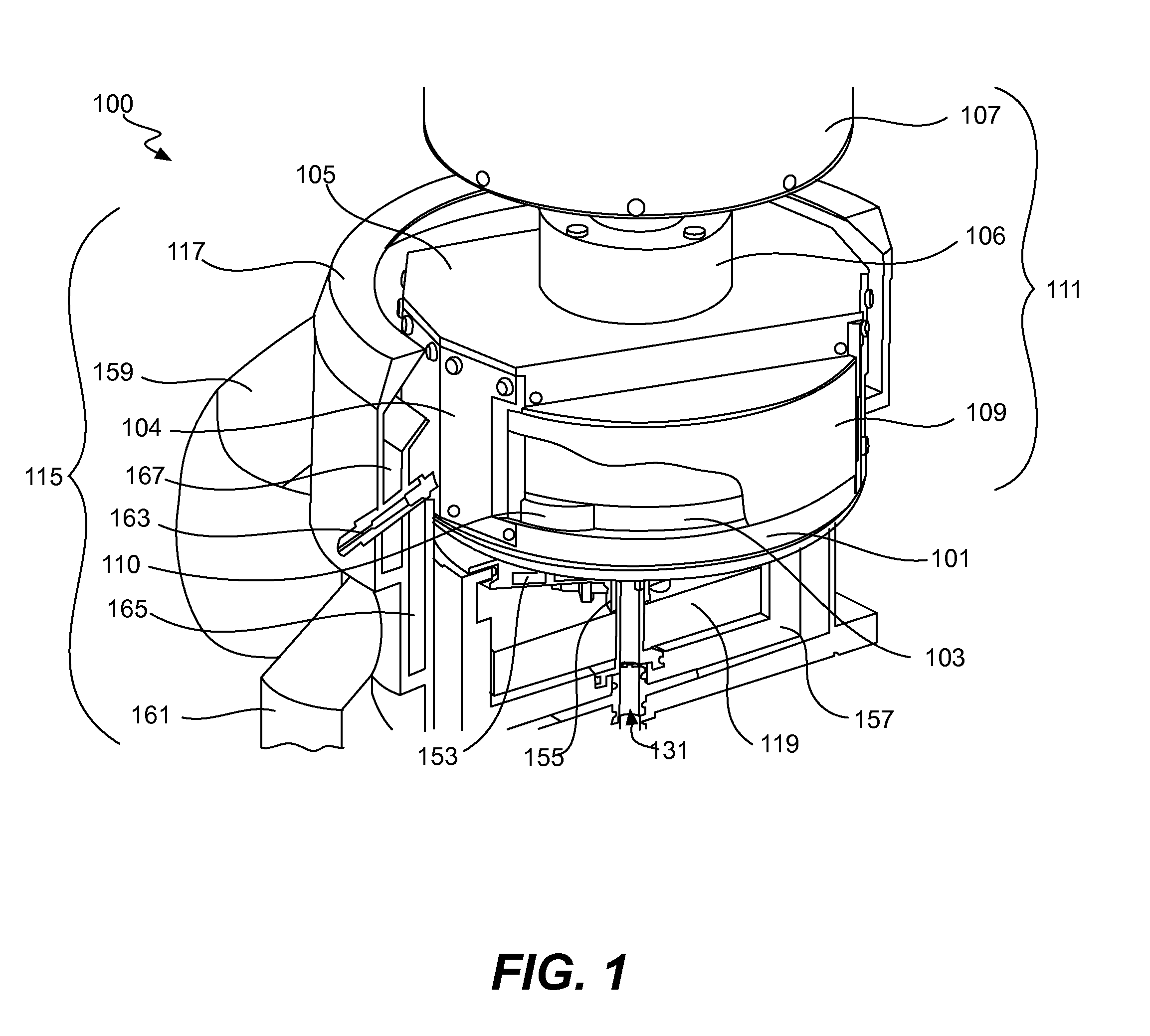
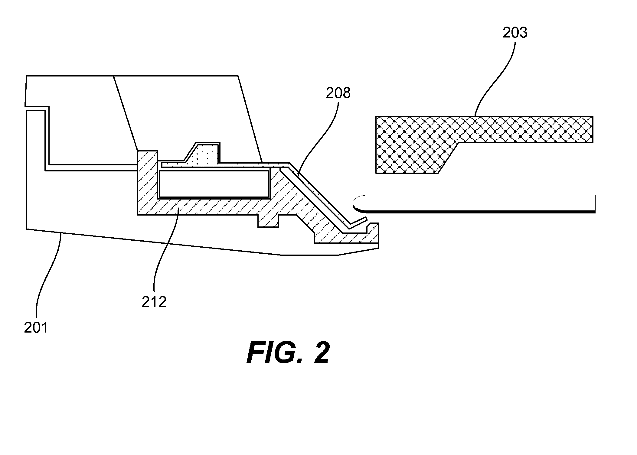
[0037]An exemplary electroplating apparatus is presented in FIG. 1 in order to provide some context for the various lipseal and contact element embodiments disclosed herein. Specifically, FIG. 1 presents a perspective view of a wafer holding and positioning apparatus 100 for electrochemically treating semiconductor wafers. The apparatus 100 includes wafer-engaging components, which are sometimes referred to as “clamshell components,” or a “clamshell assembly...


PUM

PropertyMeasurementUnit
inner diametersaaaaaaaaaa
radial widthaaaaaaaaaa
average vertical heightaaaaaaaaaa

Abstract

Disclosed are cup assemblies for holding, sealing, and providing electrical power to a semiconductor substrate during electroplating which may include a cup bottom element having a main body portion and a moment arm, an elastomeric sealing element disposed on the moment arm, and an electrical contact element disposed on the elastomeric sealing element. The main body portion may be such that it does not substantially flex when a substrate is pressed against the moment arm, and it may be rigidly affixed to another feature of the cup structure. The ratio of the average vertical thickness of the main body portion to that of the moment arm may be greater than about 5. The electrical contact element may have a substantially flat but flexible contact portion disposed upon a substantially horizontal portion of the sealing element. The elastomeric sealing element may be integrated with the cup bottom element during manufacturing.

Description

CROSS-REFERENCE TO RELATED APPLICATIONS[0001]This application claims priority to and is a continuation-in-part of U.S. patent application Ser. No. 13 / 584,343, filed Aug. 13, 2012, and titled “LIPSEALS AND CONTACT ELEMENTS FOR SEMICONDUCTOR ELECTROPLATING APPARATUSES,” which claims priority to U.S. Provisional Patent Application No. 61 / 523,800, filed Aug. 15, 2011, and titled “LIPSEALS AND CONTACT ELEMENTS FOR SEMICONDUCTOR ELECTROPLATING APPARATUSES.”[0002]This application also claims priority to U.S. Provisional Patent Application No. 62 / 085,171, filed Nov. 26, 2014, and titled “INTEGRATED LIPSEAL AND ELECTRICAL CONTACTS FOR WAFER PLATING.”[0003]Each of the foregoing patent applications are hereby incorporated by reference in their entirety and for all purposes.TECHNICAL FIELD[0004]This invention relates to the formation of damascene interconnects for integrated circuits, and electroplating apparatuses which are used during integrated circuit fabrication.BACKGROUND[0005]Electroplat...

Claims


Application Information

Patent Timeline
Patent Type & Authority Applications(United States)
IPC IPC(8): C25D17/06C25D7/12
CPCC25D17/06C25D7/12Y10T29/49778C25D17/001C25D17/004C25D7/123C25D17/005
Inventor FENG, JINGBINSTOWELL, ROBERT MARSHALLGHONGADI, SHANTINATHRAMESH, ASHWIN
Owner NOVELLUS SYSTEMS
Why Eureka
Try Eureka