Method for forming memory device

Active Publication Date: 2015-10-08
WINBOND ELECTRONICS CORP
View PDF5 Cites 17 Cited by
  • Summary
  • Abstract
  • Description
  • Claims
  • Application Information

AI Technical Summary

Benefits of technology

[0008]In accordance with one embodiment of the disclosure, a method for forming a memory device is provided. The method includes forming a resistance-switching layer over a first electrode and forming a second electrode over the resistance-switching layer. The method also includes applying a forming voltage to the resistance-switching layer such that the resistance of the resistance-switching layer is decreased. Afterwards, the method includes applying an initial reset voltage to the first electrode or the second electrode layer such that the resistance of the resistance-switching layer is increased. Afterwar

Problems solved by technology

However, since the size of the devices continues to shrink, flash memory devices have encountered issues such as high operation voltages, slow operation speeds, and bad data

Method used


Image

  • Method for forming memory device
  • Method for forming memory device
  • Method for forming memory device

Examples


Example

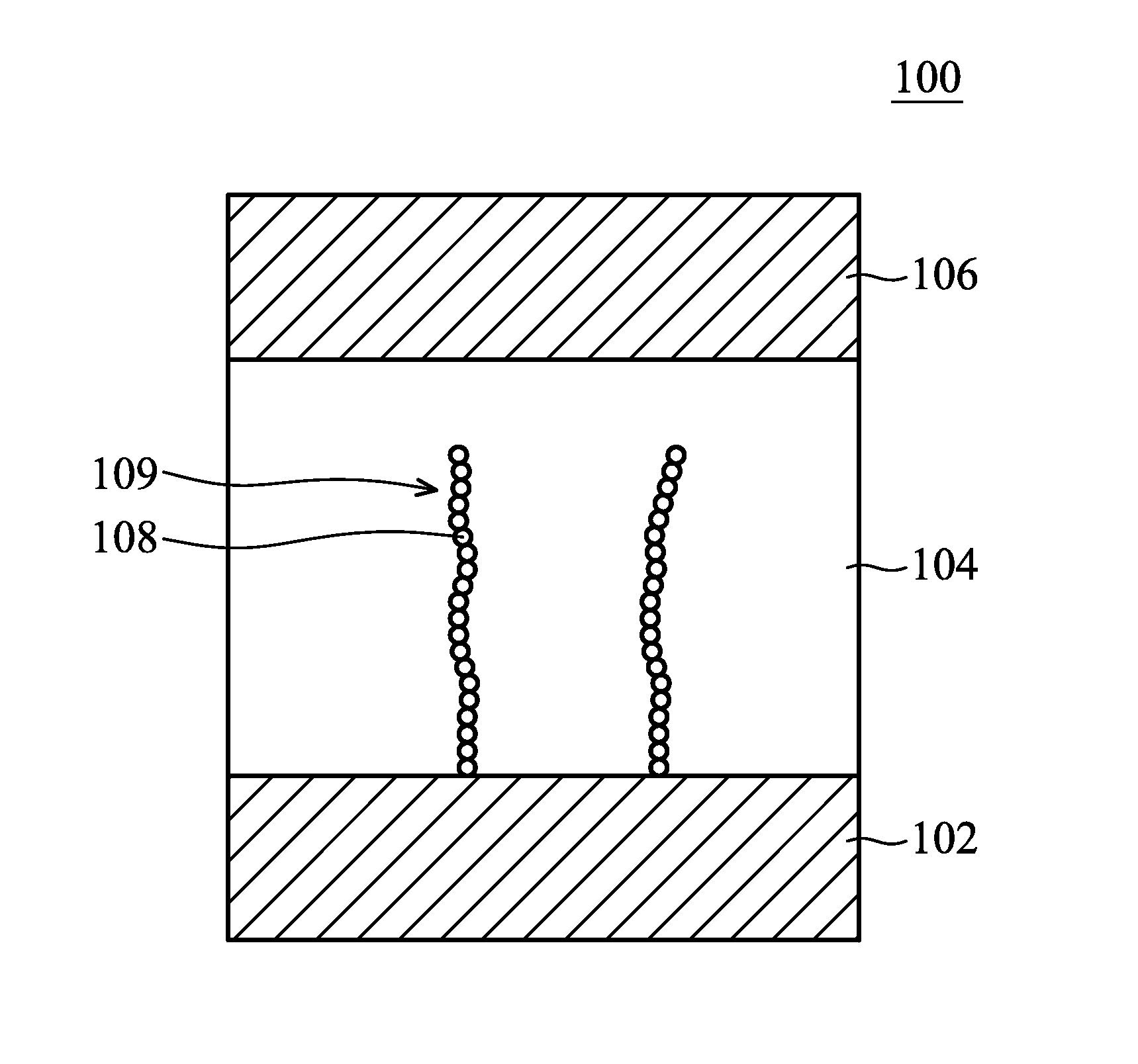
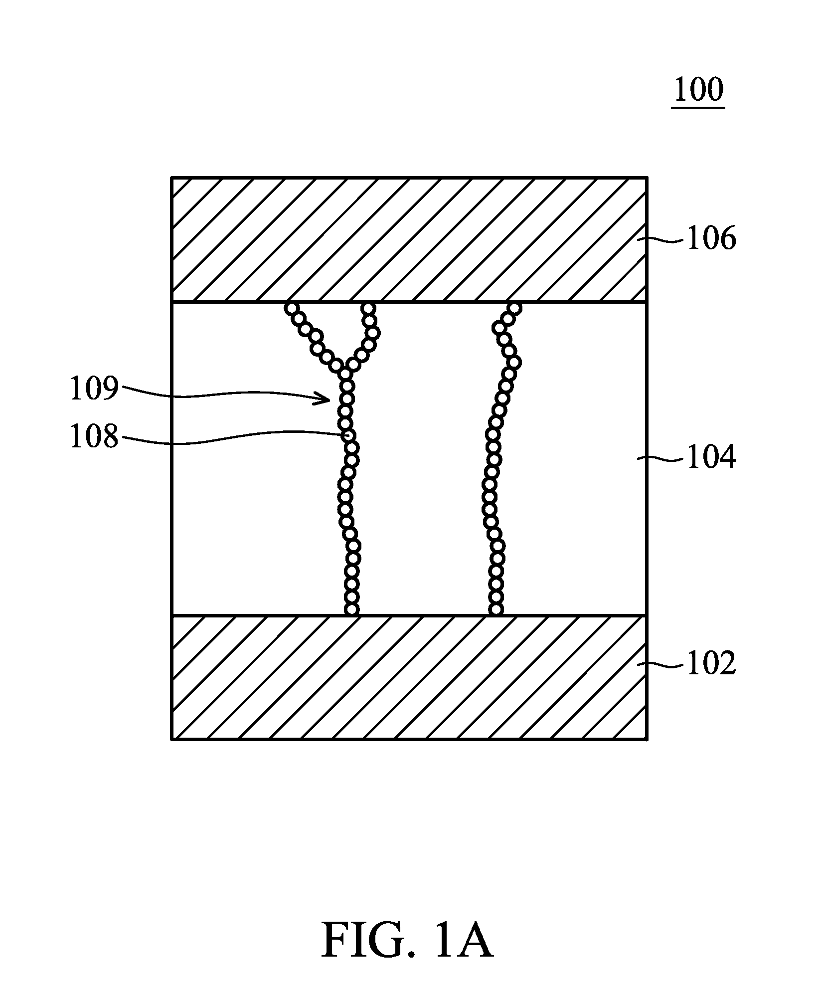
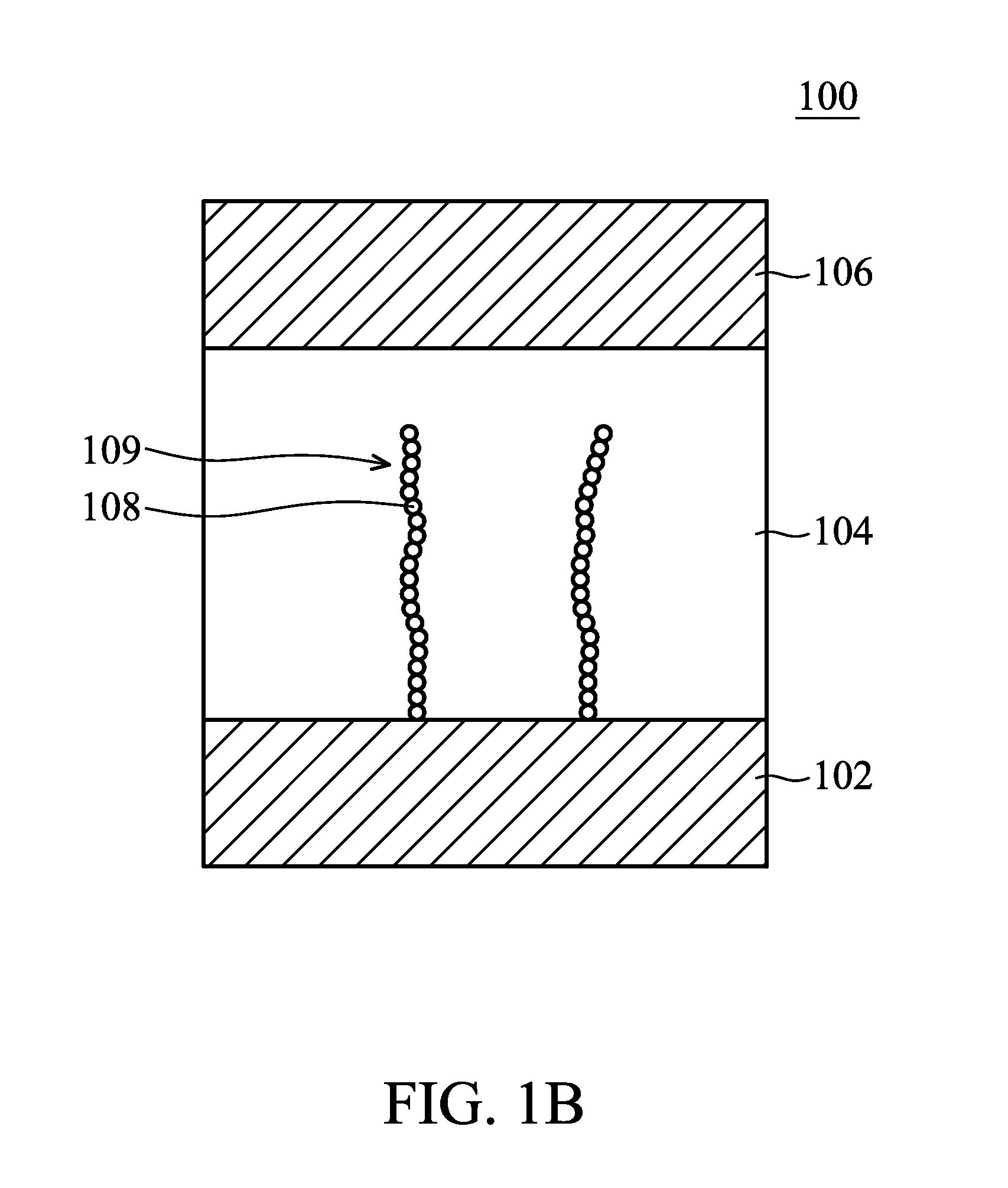
[0019]The making and using of the embodiments of the disclosure are discussed in detail below. It should be appreciated, however, that the embodiments can be embodied in a wide variety of specific contexts. The specific embodiments discussed are merely illustrative, and do not limit the scope of the disclosure.

[0020]Moreover, the performance of a first process before a second process in the description that follows may include embodiments in which the second process is performed immediately after the first process, and may also include embodiments in which additional processes may be performed between the first and second processes. Various features may be arbitrarily drawn in different scales for the sake of simplicity and clarity. Furthermore, the formation of a first material over or on a second material in the description that follows include embodiments in which the first and second materials are formed in direct contact, and may also include embodiments in which additional mat...


PUM


Abstract

A method includes forming a resistance-switching layer and a second electrode over a first electrode. The method includes applying a forming voltage to the resistance-switching layer such that the resistance of the resistance-switching layer is decreased. The method includes applying an initial reset voltage to the first electrode or the second electrode such that the resistance of the resistance-switching layer is increased. The method includes applying a first set voltage to the first electrode or the second electrode such that the resistance of the resistance-switching layer is decreased. The method includes applying a second reset voltage to first electrode or the second electrode such that the resistance of the resistance-switching layer is increased. The method includes applying a second set voltage to first electrode or the second electrode such that the resistance of the resistance-switching layer is decreased. The second set voltage is lower than the first set voltage.

Description

CROSS REFERENCE TO RELATED APPLICATIONS[0001]This Application claims priority of Taiwan Patent Application No. 103112803, filed on Apr. 08, 2014, the entirety of which is incorporated by reference herein.BACKGROUND[0002]1. Field of the Disclosure[0003]The disclosure relates to structures and formation methods of memory devices, and in particular to structures and formation methods of resistive random-access memory (RRAM) devices.[0004]2. Description of the Related Art[0005]Recently, a variety of consumer electronic products have become popular, increasing the demand for non-volatile memory devices. Flash memory is one of the mainstream non-volatile memory devices. However, since the size of the devices continues to shrink, flash memory devices have encountered issues such as high operation voltages, slow operation speeds, and bad data retention ability. As a result, future development of the flash memory device is limited.[0006]Therefore, many materials and apparatuses of new type n...

Claims


Application Information

Patent Timeline
IPC IPC(8): H01L45/00
CPCH01L45/1641H01L45/1233H01L45/146G11C2013/0083G11C13/0069G11C2213/15H10N70/24H10N70/8833H10N70/826H10B63/00H10B63/20H10N70/041
Inventor LIN, MENG-HENGWU, BO-LUN
Owner WINBOND ELECTRONICS CORP
Why Eureka
Try Eureka