Active matrix substrate, x-ray imaging panel including same, and producing method thereof

Inactive Publication Date: 2019-08-22
SHARP KK
View PDF8 Cites 0 Cited by
  • Summary
  • Abstract
  • Description
  • Claims
  • Application Information

AI Technical Summary

Benefits of technology

[0008]According to the above configuration, detection defect

Problems solved by technology

As a result, the bias line has a higher resistance

Method used


Image

  • Active matrix substrate, x-ray imaging panel including same, and producing method thereof
  • Active matrix substrate, x-ray imaging panel including same, and producing method thereof
  • Active matrix substrate, x-ray imaging panel including same, and producing method thereof

Examples


embodiment 1

(Configuration)

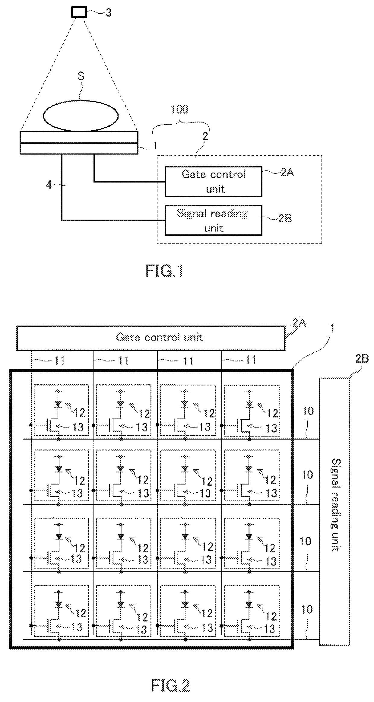
[0067]FIG. 1 schematically illustrates an X-ray imaging device in the present embodiment. The X-ray imaging device 100 includes an active matrix substrate 1 and a control unit 2. The control unit 2 includes a gate control unit 2A and a signal reading unit 2B. X-rays are projected from the X-ray source 3 to an object S, and X-rays transmitted through the object S are converted into fluorescence (hereinafter referred to as scintillation light) by a scintillator 4 provided above the active matrix substrate 1. The X-ray imaging device 100 picks up the scintillation light with the active matrix substrate 1 and the control unit 2, thereby acquiring an X-ray image.

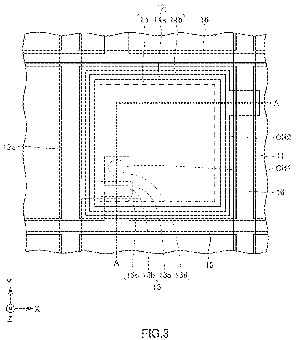
[0068]FIG. 2 is a schematic diagram showing a schematic configuration of the active matrix substrate 1. As shown in FIG. 2, a plurality of source lines 10, and a plurality of gate lines 11 intersecting with the source lines 10 are formed in the active matrix substrate 1. The gate lines 11 are connected with the gat...

embodiment 2

[0126]As the present embodiment, a method for producing the active matrix substrate 1 of Embodiment 1, which is different from the method of Embodiment 1, is described. The following description describes steps different from those in Embodiment 1.

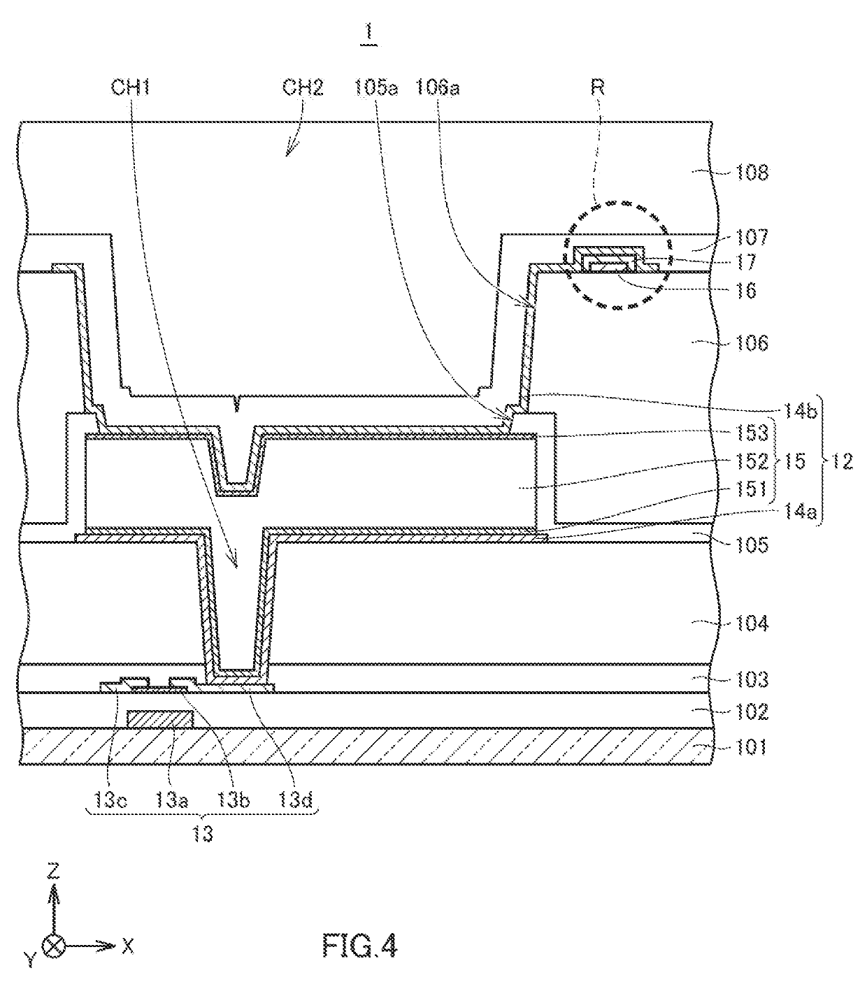
[0127]After the steps shown in FIGS. 6A to 6I, the opening 105a of the third insulating film 105 is formed in Embodiment 1; in the present embodiment, however, the step shown in FIG. 6I is subsequently followed by a step of forming the fourth insulating film 106 by using, for example, slit coating (see FIG. 7A).

[0128]Thereafter, photolithography and wet etching are carried out so that the opening 106a of the fourth insulating film 106 is formed on the photoelectric conversion layer 15 (see FIG. 7B).

[0129]Subsequently, photolithography and wet etching are carried out so that the opening 105a of the third insulating film 105 is formed on an inner side with respect to the opening 106a of the fourth insulating film 106. Here, for wet etching, ...

embodiment 3

[0133]As the present embodiment, a method for producing the active matrix substrate 1 of Embodiment 1, which is different from the method of Embodiment 2, is described. The following description describes steps different from those in Embodiment 2.

[0134]In Embodiment 2 described above, the opening 105a of the third insulating film 105 is formed after the step shown in FIG. 7B; in the present embodiment, however, after the step shown in FIG. 7B, the metal film 160 obtained by laminating molybdenum-niobium (MoNb), aluminum (Al), and molybdenum-niobium (MoNb) sequentially in this order by using, for example, sputtering is formed on the third insulating film 105 and the fourth insulating film 106 (see FIG. 8A).

[0135]Subsequently, photolithography and wet etching are carried out so as to pattern the metal film 160. Through these steps, the bias line 16 is formed on an outer side with respect to the photoelectric conversion layer 15, on the fourth insulating film 106 (see FIG. 8B).

[0136]T...


PUM


Abstract

Provided is a technique with which detection defects due to a higher resistance of bias lines can be suppressed. An active matrix substrate 1 has a plurality of detection circuitry arranged in matrix. Each of the detection circuitry includes a photoelectric conversion layer 15; a pair of a first electrode 14a and a second electrode 14b between which the photoelectric conversion layer 15 is interposed; an insulating film 106 covering a side end portion of the photoelectric conversion layer 15; a bias line 16 that is provided on the insulating film 106, and applies a bias voltage to the second electrode 14b; and a protection film 17 that is provided on the insulating film 106, covers a surface of the bias line 16, and contains a conductive material having resistance against acid. At least at a part of the second electrode 14b covers the protection film 17.

Description

TECHNICAL FIELD[0001]The present invention relates to an active matrix substrate, an X-ray imaging panel including the same, and a method for producing the same.BACKGROUND ART[0002]Conventionally, an X-ray imaging device is known that includes thin film transistors (also referred to as “TFTs”) in a plurality of areas arranged in matrix (hereinafter referred to as pixel portions), and picks up an image of irradiated X-rays with a plurality of pixel portions. In such an X-ray imaging device, for example, p-intrinsic-n (PIN) photodiodes are used as photoelectric conversion elements that convert irradiated X-rays into charges. The converted charges are read out by causing the TFTs of the respective pixels to operate. With the charges being read out in this way, an X-ray image is obtained.[0003]Patent Document 1 discloses such an X-ray imaging device. More specifically, in the configuration disclosed in Patent Document 1, of a pair of electrodes between which the photodiode is interposed...

Claims


Application Information

Patent Timeline
IPC IPC(8): H01L27/146H01L21/02H01L31/20H01L31/0376H01L31/105G01T1/20
CPCH01L27/14636H01L27/1462H01L27/14663H01L27/14612H01L27/14685H01L21/02057H01L27/14692H01L31/202H01L27/14689H01L31/03762H01L31/1055G01T1/2018H01L27/14658H01L27/14609G01T1/20184H01L27/14603H01L31/022408H01L31/115H01L31/035281Y02E10/548
Inventor MISAKI, KATSUNORI
Owner SHARP KK
Why Eureka
Try Eureka