Array substrate, manufacturing method thereof and display device

a technology of array substrate and manufacturing method, applied in non-linear optics, instruments, optics, etc., can solve the problem of low brightness of thin film transistor liquid crystal display, and achieve the effect of improving the aperture ratio of the array substra

Active Publication Date: 2016-01-07
BOE TECH GRP CO LTD +1
View PDF4 Cites 19 Cited by
  • Summary
  • Abstract
  • Description
  • Claims
  • Application Information

AI Technical Summary

Benefits of technology

The present invention provides an improved design for an array substrate that increases its aperture ratio. This improvement involves placing two layers of thin film transistors (TFTs) on top of each other in a way that reduces their size and interference with neighboring components. By doing this, the TFTs can be arranged more efficiently without compromising performance or reliability.

Problems solved by technology

The technical problem addressed in this patent relates to improving the layout of the array substrate in thin film transistor liquid crystal displays to increase the aperture ratio and enhance their brightness while reducing the number of wirings needed.

Method used


Image

  • Array substrate, manufacturing method thereof and display device
  • Array substrate, manufacturing method thereof and display device
  • Array substrate, manufacturing method thereof and display device

Examples


Embodiment Construction

[0060]In order to make objects, technical details and advantages of the embodiments of the invention apparent, the technical solutions of the embodiment will be described in a clearly and fully understandable way in connection with the drawings related to the embodiments of the invention. It is obvious that the described embodiments are just a part but not all of the embodiments of the invention. Based on the described embodiments herein, those skilled in the art can obtain other embodiment(s), without any inventive work, which should be within the scope of the invention.

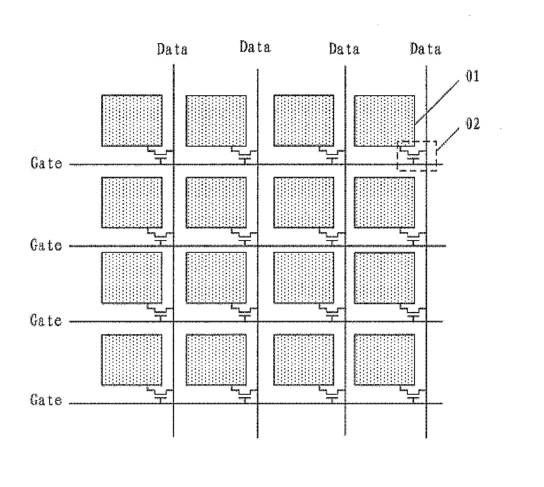
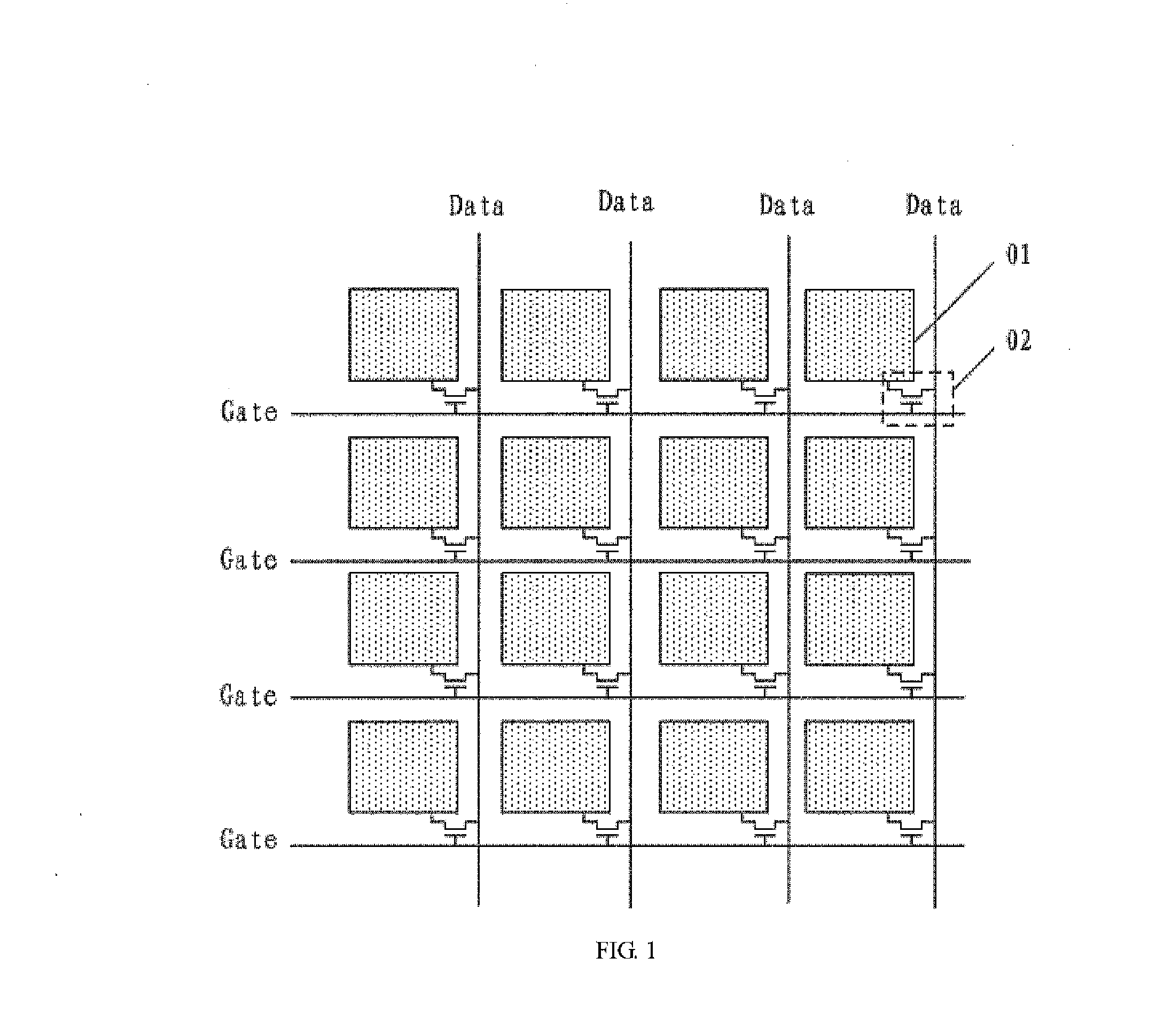
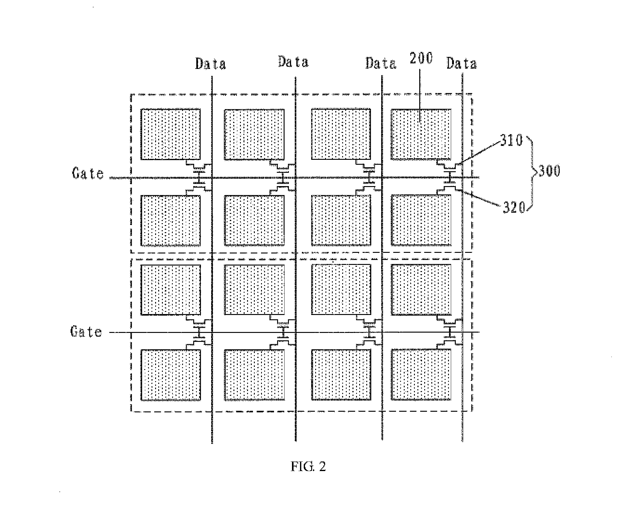
[0061]Sizes and shapes of respective parts in the accompanying drawings do not reflect true proportions of the array substrate, but only aim to illustrate content of the present invention.

[0062]An embodiment of the present invention provides an array substrate, as illustrated in FIG. 2, comprising a base substrate (not illustrated), and a plurality of pixel units 200 arranged in a matrix which have pixel electrodes ...


PUM


Abstract

An array substrate, a manufacturing method thereof and a display device are provided; in the array substrate, two adjacent rows of the pixel units (200) are taken as a group of pixel unit rows; in each group of the pixel unit rows, since the pixel electrodes in two adjacent pixel units (200) of a same column are all electrically connected with one composite transistor (300), and the composite transistor (300) can be turned on or off under the control of different levels of control voltages, to charge the pixel electrodes in two adjacent pixel units (200) of the same column at different times, each group of the pixel unit row can share a gate line located between the two rows of the pixel units, as compared with the conventional array substrate, the number of the gate lines disposed on the array substrate is reduced by half, so that the aperture ratio of the array substrate can be improved, and the brightness of the display panel can be further improved.

Description


Claims


Application Information

Patent Timeline
Owner BOE TECH GRP CO LTD
Why Eureka
Try Eureka