N-Path Interleaving Analog-to-Digital Converter (ADC) with Offset gain and Timing Mismatch Calibration

Active Publication Date: 2016-02-18
IQ ANALOG
View PDF0 Cites 17 Cited by
  • Summary
  • Abstract
  • Description
  • Claims
  • Application Information

AI Technical Summary

Benefits of technology

[0016]In a parallel second process, the interleaved ADC signal is delayed, creating a delayed signal. The rotated signal is multiplied by the delayed signal to create a timing error signal. Using the timing error signal, timing errors are accumulated for the ADC signal paths, and corrections are applied that minimize timing errors in each of the n ADC signal paths.

Problems solved by technology

As a result these timing and gain errors produce artifacts which in frequency domain show up as spectral images of the desired signal centered around every multiple of fs / n, where fs is the sampling rate of the composite ADC.

Method used


Image

  • N-Path Interleaving Analog-to-Digital Converter (ADC) with Offset gain and Timing Mismatch Calibration
  • N-Path Interleaving Analog-to-Digital Converter (ADC) with Offset gain and Timing Mismatch Calibration
  • N-Path Interleaving Analog-to-Digital Converter (ADC) with Offset gain and Timing Mismatch Calibration

Examples


Embodiment Construction

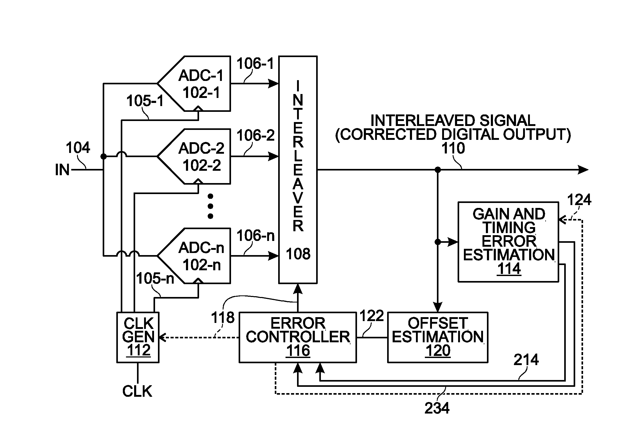
[0032]FIG. 1 is a schematic block diagram of an n-path time interleaved analog-to-digital converter (ADC) with a system for calibrating timing mismatch. The ADC 100 comprises at least n ADCs 102-1 through 102-n. Each ADC has an input on line 104 to accept the analog input, and input on lines 105-1 through 105-n to accept clock signals, and an output path, respectively 106-1 through 106-n, to supply a. digital sample signal, where n is an integer greater than 1. An interleaver 108 has inputs to accept the digital sample signals on lines 106-1 through 106-n, and an output on line 110 to supply a digital n-path interleaved ADC signal. Since this path occurs after error correction, it may also be known as a corrected digital output. A clock 112 is also shown to provide n number of different phases of the sampling clock fs to the ADCs 102-1 through 102-n. The ADC 100 further comprises a gain and timing error estimation block 114. Offset estimation block 120 accepts the interleaved ADC si...


PUM


Abstract

A system and method are provided for calibrating timing mismatch in an n-path time interleaved analog-to-digital converter (ADC). The method digitizes an analog signal with an n-path interleaved ADC, creating an interleaved ADC signal. In a first process, the phase of the interleaved ADC signal is rotated by 90 degrees, creating a rotated signal. This rotation may be accomplished using a finite impulse response (FIR) filter with taps at {0.5, 0, −0.5}, enabled as a derivative filter, or as a Hilbert transformation. In a parallel second process, the interleaved ADC signal is delayed, creating a delayed signal. The rotated signal is multiplied by the delayed signal to create a timing error signal. Using the timing error signal, timing errors are accumulated for the ADC signal paths, and corrections are applied that minimize timing errors in each of the n ADC signal paths.

Description

RELATED APPLICATIONS[0001]The following applications are incorporated herein by reference:[0002]CURRENT IMPULSE (CI) DIGITAL-TO-ANALOG CONVERTER (DAC), invented by Mikko Waltari, Ser. No. 141750,203, filed Jun. 25, 2015, filed Jun. 25, 2015, issued as U.S. Pat. No. 9,178,528[0003]TRAVELING PULSE WAVE QUANTIZER, invented by Mikko Waltari, Ser. No. 14 / 681,206, filed Apr. 8, 2015; issued as U.S. Pat. No. 9,098,072;[0004]N-PATH INTERLEAVING ANALOG-TO-DIGITAL CONVERTER (ADC) WITH BACKGROUND CALIBRATION, invented by Mikko Waltari, Ser. No. 14 / 531,371, filed Nov. 3, 2014, now U.S. Pat. No. 9.030,340;[0005]INTERLEAVING ANALOG-TO-DIGITAL CONVERTER (ADC) WITH BACKGROUND CALIBRATION, invented by Mikko Waltari et al., Ser. No. 14 / 511,206, filed Oct. 10, 2014, now U.S. Pat. No. 8,917,125;[0006]SYSTEM AND METHOD FOR FREQUENCY MULTIPLIER JITTER CORRECTION, invented by Mikko Waltari et al., Ser. No. 14 / 081,568, filed Nov. 15, 2013, now U.S. Pat. No. 8,878,577;[0007]TIME-INTERLEAVED ANALOG-TO-DIGITA...

Claims


Application Information

Patent Timeline
Patent Type & Authority Applications(United States)
IPC IPC(8): H03M1/10H03M1/12
CPCH03M1/1023H03M1/121H03M1/1245H03M1/0626H03M1/0836H03M1/1052H03M1/1215
Inventor WALTARI, MIKKO
Owner IQ ANALOG
Why Eureka
Try Eureka