Photographing optical lens assembly, imaging device and electronic device

a technology of optical lenses and optical lenses, applied in the field of compact photographing optical lens assemblies and imaging devices, can solve the problems of poor image quality, inability to easily suppress the angle of light projected onto the sensor, etc., and achieve the effect of effectively suppressing the incident angle of light projected and improving light convergen

Active Publication Date: 2016-05-26
LARGAN PRECISION
View PDF7 Cites 9 Cited by
  • Summary
  • Abstract
  • Description
  • Claims
  • Application Information

AI Technical Summary

Benefits of technology

[0007]According to one aspect of the present disclosure, a photographing optical lens assembly includes, in order from an object side to an image side, a first lens element, a second lens element, a third lens element and a fourth lens element. The fourth lens element has an object-side surface being concave in a paraxial region thereof and an image-side surface being convex in a paraxial region thereof ...

Problems solved by technology

However, the incident angle of light projected onto the sensor cannot be...

Method used


Image

  • Photographing optical lens assembly, imaging device and electronic device
  • Photographing optical lens assembly, imaging device and electronic device
  • Photographing optical lens assembly, imaging device and electronic device

Examples


1st embodiment

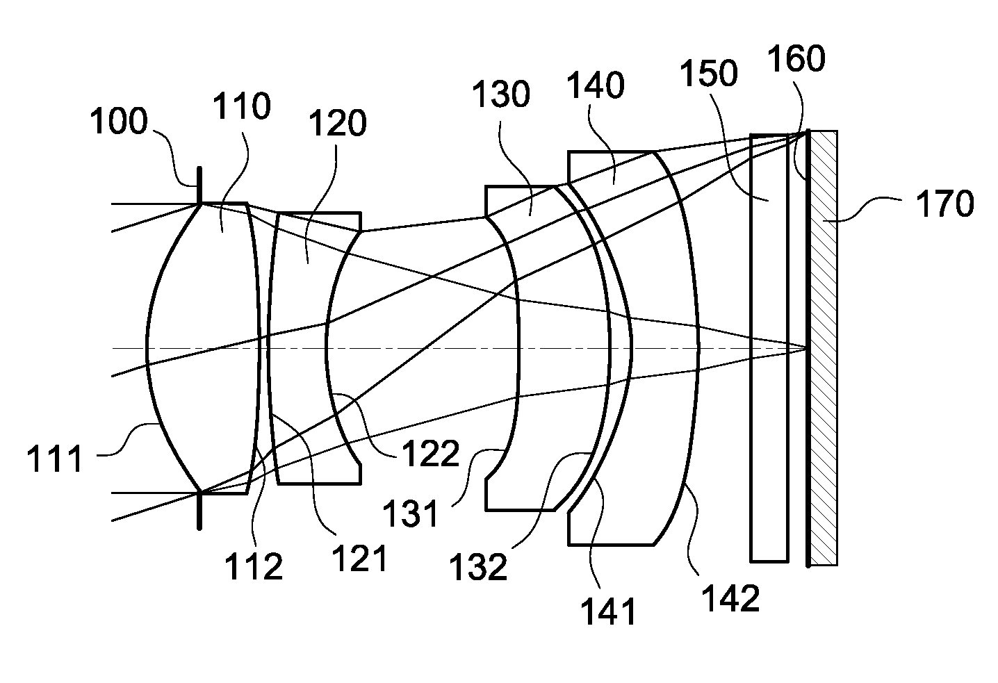
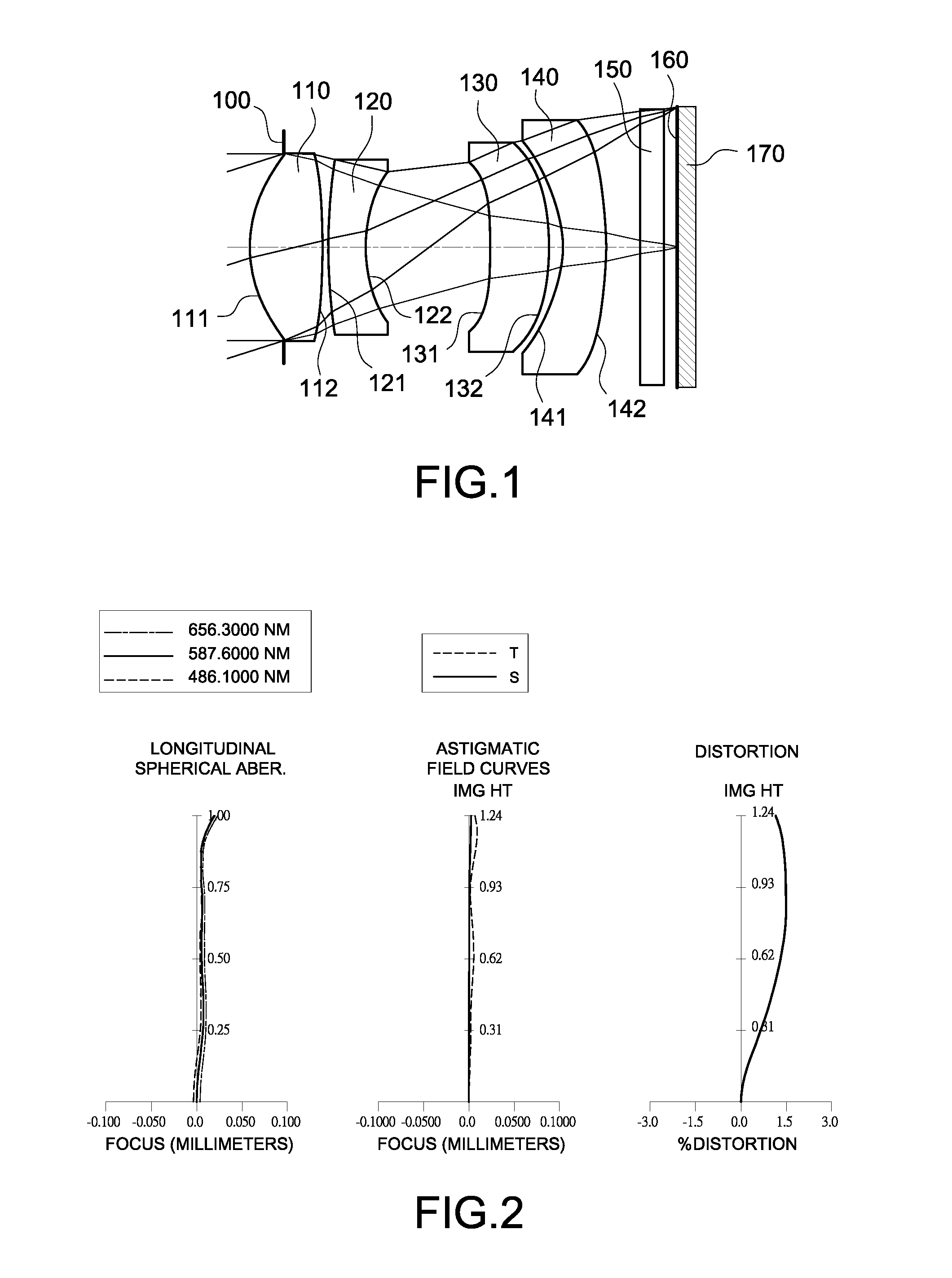
[0060]FIG. 1 is a schematic view of an imaging device according to the 1st embodiment of the present disclosure. FIG. 2 shows spherical aberration curves, astigmatic field curves and a distortion curve of the imaging device according to the 1st embodiment. In FIG. 1, the imaging device includes a photographing optical lens assembly (its reference numeral is omitted) and an image sensor 170. The photographing optical lens assembly includes, in order from an object side to an image side, an aperture stop 100, a first lens element 110, a second lens element 120, a third lens element 130, a fourth lens element 140, a filter 150 and an image surface 160, wherein the image sensor 170 is located at the image surface 160 of the photographing optical lens assembly. The photographing optical lens assembly has a total of four lens elements (110-140) with refractive power, and there is an air gap in a paraxial region between any two of the first lens element 110, the second lens element 120, th...

2nd embodiment

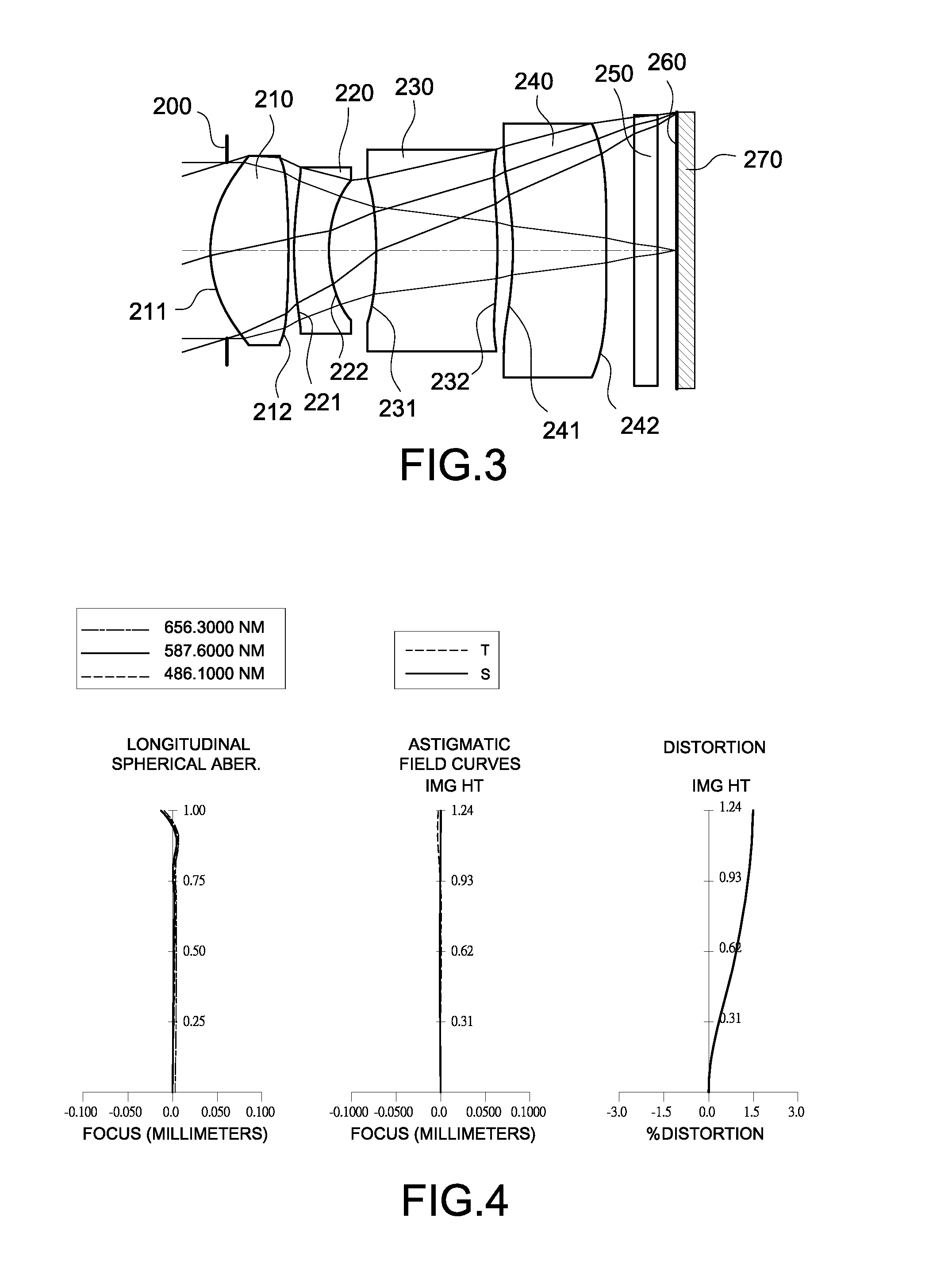
[0087]FIG. 3 is a schematic view of an imaging device according to the 2nd embodiment of the present disclosure. FIG. 4 shows, in order from left to right, spherical aberration curves, astigmatic field curves and a distortion curve of the imaging device according to the 2nd embodiment. In FIG. 3, the imaging device includes a photographing optical lens assembly (its reference numeral is omitted) and an image sensor 270. The photographing optical lens assembly includes, in order from an object side to an image side, an aperture stop 200, a first lens element 210, a second lens element 220, a third lens element 230, a fourth lens element 240, a filter 250 and an image surface 260, wherein the image sensor 270 is located at the image surface 260 of the photographing optical lens assembly. The photographing optical lens assembly has a total of four lens elements (210-240) with refractive power, and there is an air gap in a paraxial region between any two of the first lens element 210, t...

3rd embodiment

[0096]FIG. 5 is a schematic view of an imaging device according to the 3rd embodiment of the present disclosure. FIG. 6 shows, in order from left to right, spherical aberration curves, astigmatic field curves and a distortion curve of the imaging device according to the 3rd embodiment. In FIG. 5, the imaging device includes a photographing optical lens assembly (its reference numeral is omitted) and an image sensor 370. The photographing optical lens assembly includes, in order from an object side to an image side, an aperture stop 300, a first lens element 310, a second lens element 320, a third lens element 330, a fourth lens element 340, a filter 350 and an image surface 360, wherein the image sensor 370 is located at the image surface 360 of the photographing optical lens assembly. The photographing optical lens assembly has a total of four lens elements (310-340) with refractive power, and there is an air gap in a paraxial region between any two of the first lens element 310, t...


PUM


Abstract

A photographing optical lens assembly includes, in order form an object side to an image side, a first lens element, a second lens element, a third lens element, and a fourth lens element. The first lens element with positive refractive power has an object-side surface being convex in a paraxial region. The second lens element has negative refractive power. The third lens element with refractive power has an object-side surface being concave in a paraxial region, and the object-side surface and an image-side surface are both aspheric. The fourth lens element with negative refractive power has an object-side surface being concave in a paraxial region, and an image-side surface being convex in a paraxial region, the object-side surface and the image-side surface are both aspheric.

Description

RELATED APPLICATIONS[0001]This application claims priority to Taiwan Application Serial Number 103140891 filed Nov. 25, 2014, which is herein incorporated by reference.BACKGROUND[0002]1. Technical Field[0003]The present disclosure relates to a photographing optical lens assembly and an imaging device. More particularly, the present disclosure relates to a compact photographing optical lens assembly and imaging device applicable to electronic devices.[0004]2. Description of Related Art[0005]In recent years, with the popularity of mobile terminals having camera functionalities, the demand of miniaturized optical systems has been increasing. The sensor of a conventional optical system is typically a CCD (Charge-Coupled Device) or a CMOS (Complementary Metal-Oxide-Semiconductor) sensor. As the advanced semiconductor manufacturing technologies have reduced the pixel size of image sensors and compact optical systems have gradually evolved toward the field of higher megapixels, there is an...

Claims


Application Information

Patent Timeline
IPC IPC(8): G02B13/18H04N5/225G02B13/00
CPCG02B13/18H04N5/2254G02B13/0015G02B13/004G02B9/34
Inventor HSIEH, TUNG-YICHEN, WEI-YU
Owner LARGAN PRECISION
Why Eureka
Try Eureka