Array substrate, in-cell touch screen and touch display device
a touch display device and substrate technology, applied in the field of array substrates, can solve the problems of reducing the signal to noise ratio of the in-cell touch screen, increasing the thickness and weight of the entire display device, etc., and achieves the effects of enhancing the emission intensity of a touch signal, prolonging the boundary, and increasing the mutual capacitance between the sensing sub-electrode and the driving sub-electrod
- Summary
- Abstract
- Description
- Claims
- Application Information
AI Technical Summary
Benefits of technology
Problems solved by technology
Method used
Image
Examples
first embodiment
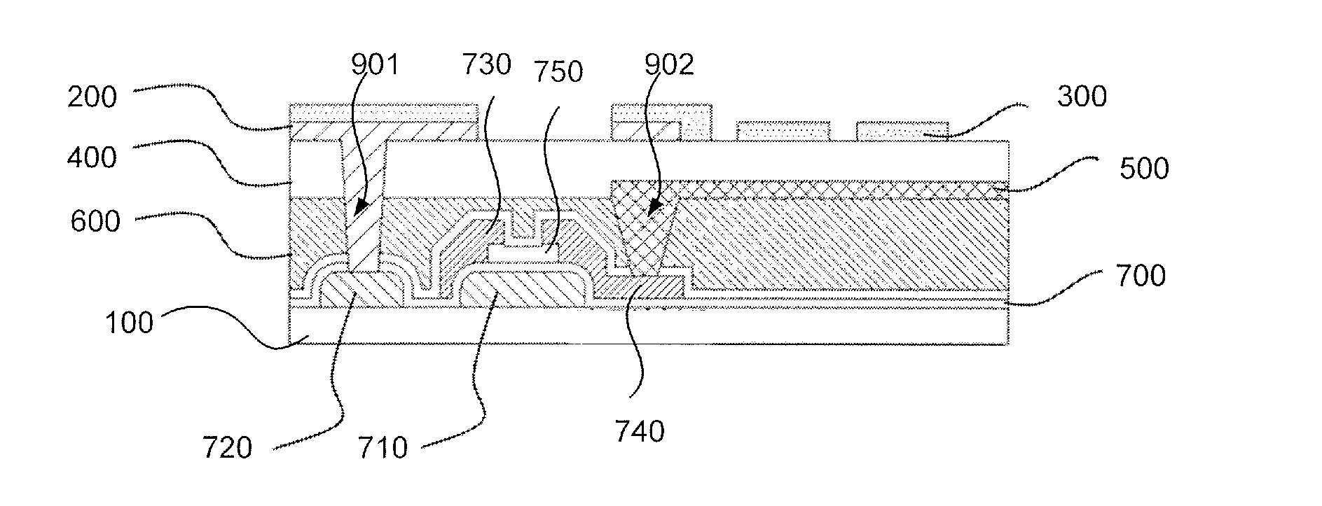
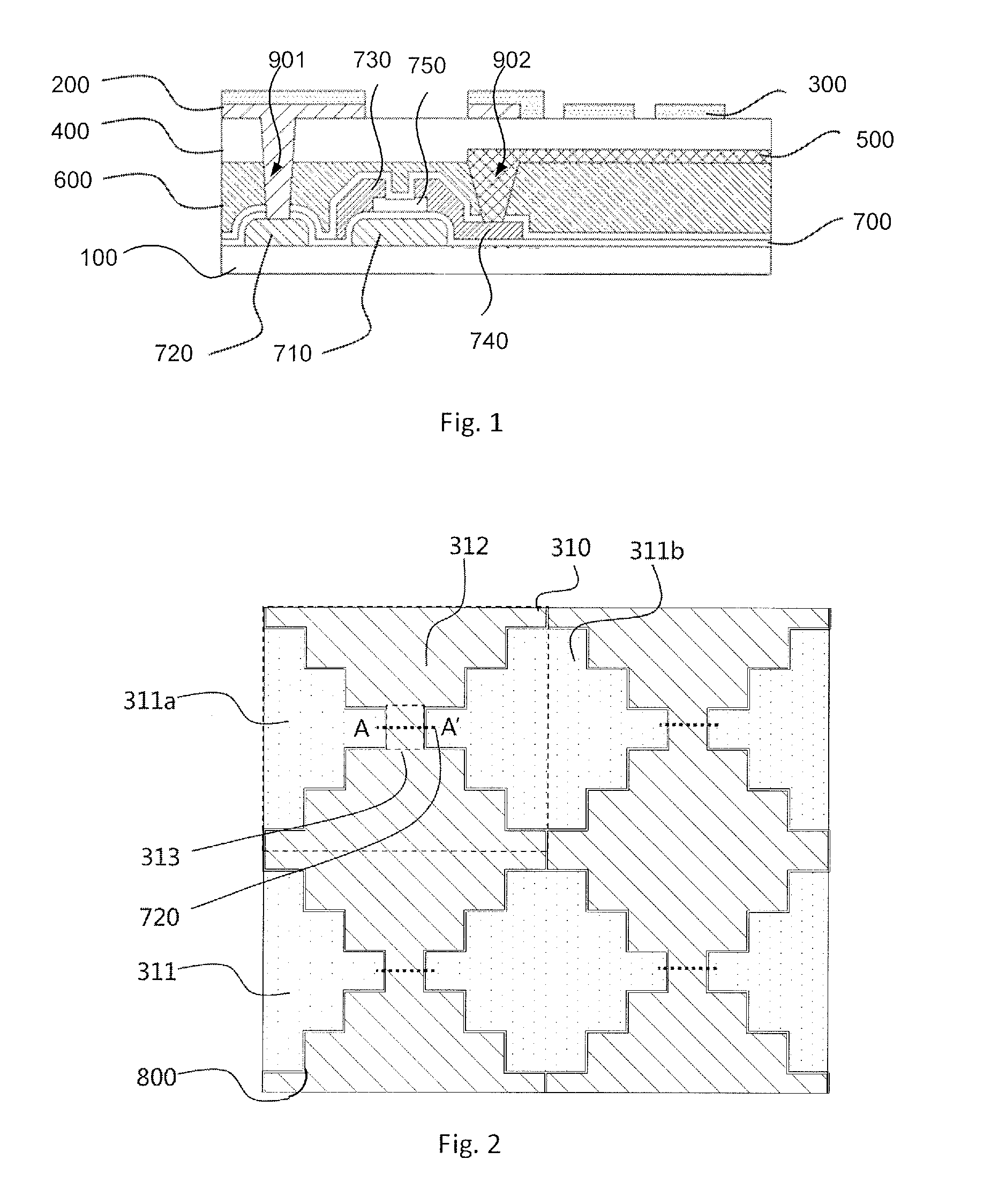
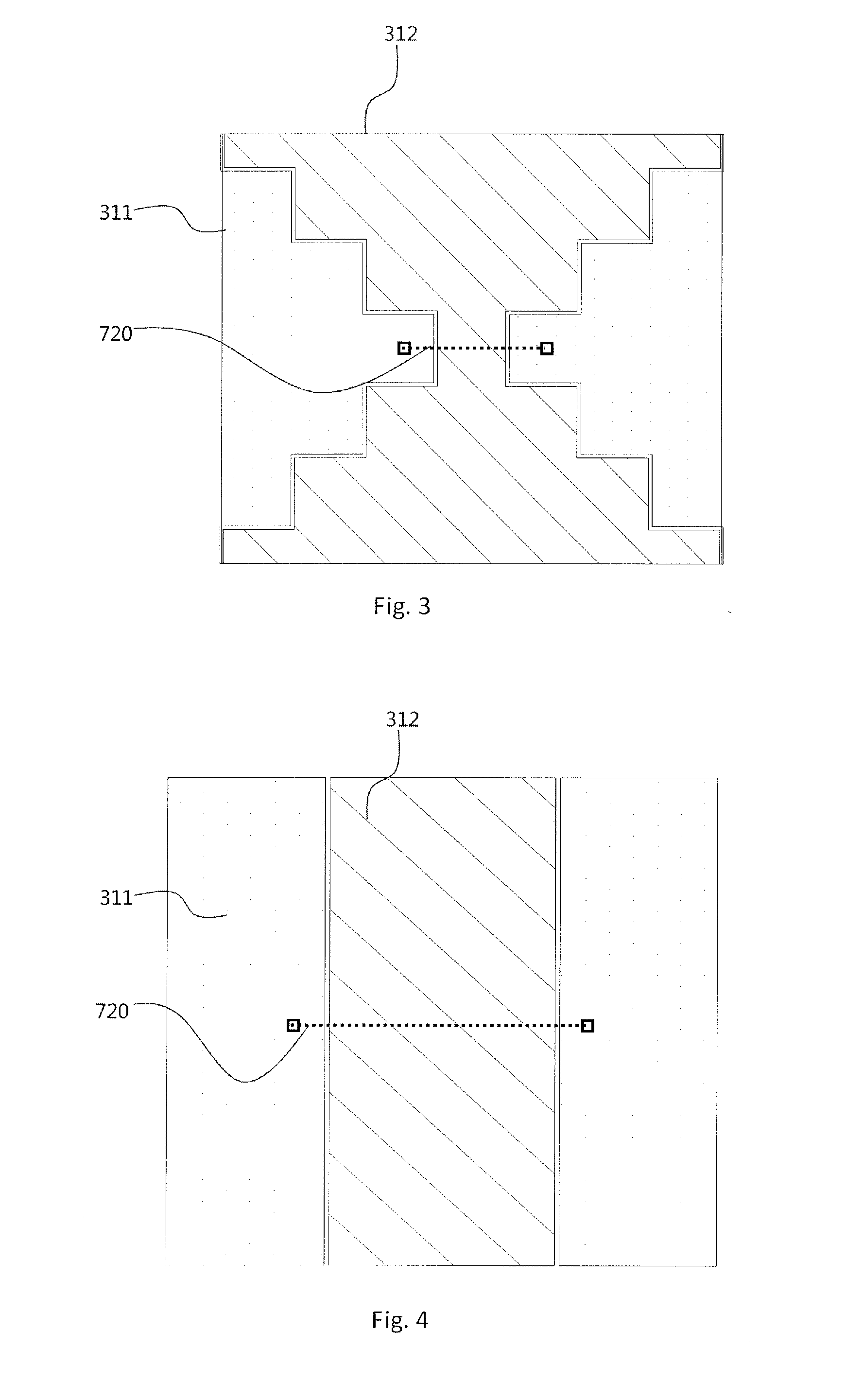
[0032]The embodiment of the invention provides an array substrate as illustrated in FIG. 1. The array substrate comprises a base substrate 100, and a gate electrode 710, a source electrode 730, a drain electrode 740 and a semiconductor layer 750 arranged on the base substrate 100, and further comprises a common electrode layer 300. The common electrode layer 300 is provided with a plurality of driving electrodes and a plurality of sensing electrodes with extending directions perpendicular to each other, wherein each of the driving electrodes includes a plurality of driving sub-electrodes which are connected to one another, each of the sensing electrodes includes a plurality of sensing sub-electrodes which are connected to one another, and adjacent driving sub-electrodes and sensing sub-electrodes have concave-convex structures in a staggered arrangement at borders and insulated from each other.
[0033]For example, the driving sub-electrode and the sensing sub-electrode have serrated e...
second embodiment
[0057]The second embodiment of the invention provides an in-cell touch screen, as illustrated in FIG. 7. The in-cell touch screen comprises a color filter substrate and the array substrate according to the first embodiment, wherein a black matrix 110 is further arranged between adjacent sub-pixel units on the color filter substrate, the driving metal wires 210, the sensing metal wires 220 as well as the borders 800 between the driving sub-electrodes 311 and the sensing sub-electrodes 312 are all corresponding to the black matrix in position, as illustrated in FIG. 8.
[0058]Therein, the color filter substrate comprises a base substrate 100, a black matrix 110 and a color filter layer 120, and it can be seen from FIG. 8 that the black matrix 110 on the color filter substrate can be corresponding to the border 800 between the a driving sub-electrode and an sensing sub-electrode on the array substrate, and can also be corresponding to a thin film transistor on the array substrate in posi...
third embodiment
[0059]The third embodiment of the invention further provides a touch display device, comprising the in-cell touch screen according to the second embodiment, which increases signal to noise ratio while realizing a touch and display function.
[0060]The touch display device provided in this embodiment may be electronic paper, a cell phone, a tablet computer, a TV set, a laptop, a digital photo frame, a navigator or any product or component with a display function.
PUM
 Abstract
Description
Claims
Application Information


