Split Gate Non-volatile Memory Cell With 3D FINFET Structure, And Method Of Making Same
- Summary
- Abstract
- Description
- Claims
- Application Information
AI Technical Summary
Benefits of technology
Problems solved by technology
Method used
Image

Examples
Embodiment Construction
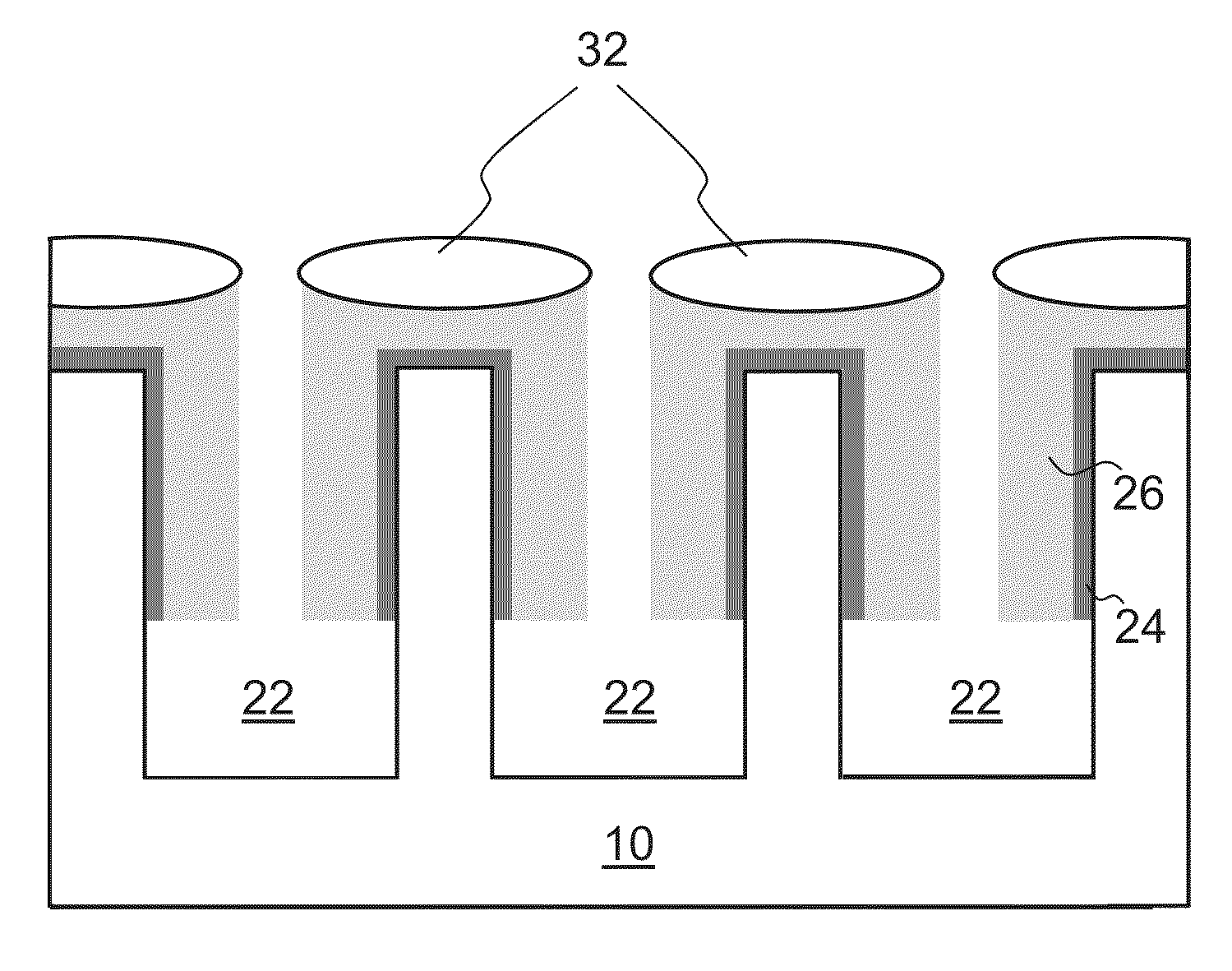
[0014]The present invention is a Fin-FET configuration for the simple split gate type memory cell that has only two gates, a floating gate and a control gate, where the control gate has a first portion laterally adjacent to the floating gate and a second portion that extends up and over the floating gate. The method of making such a split gate memory cell provide many advantages, including silicon trench etching and partial oxide fill for isolation, and self-aligned components such as the floating gate.
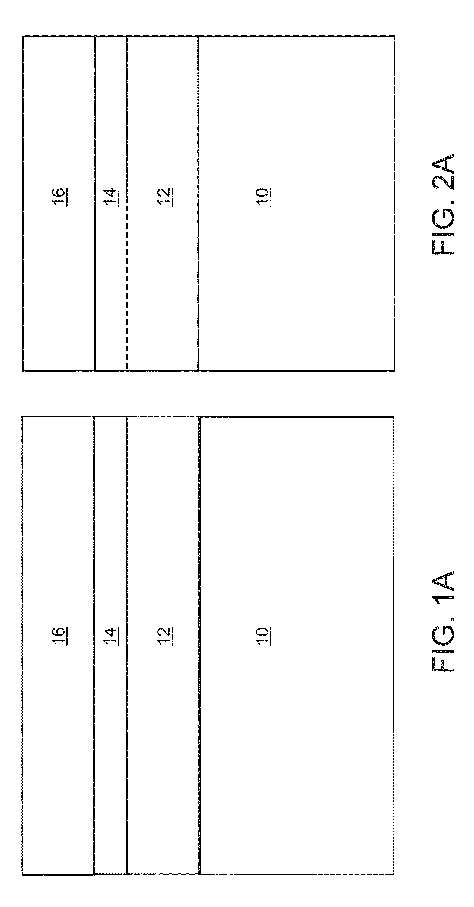
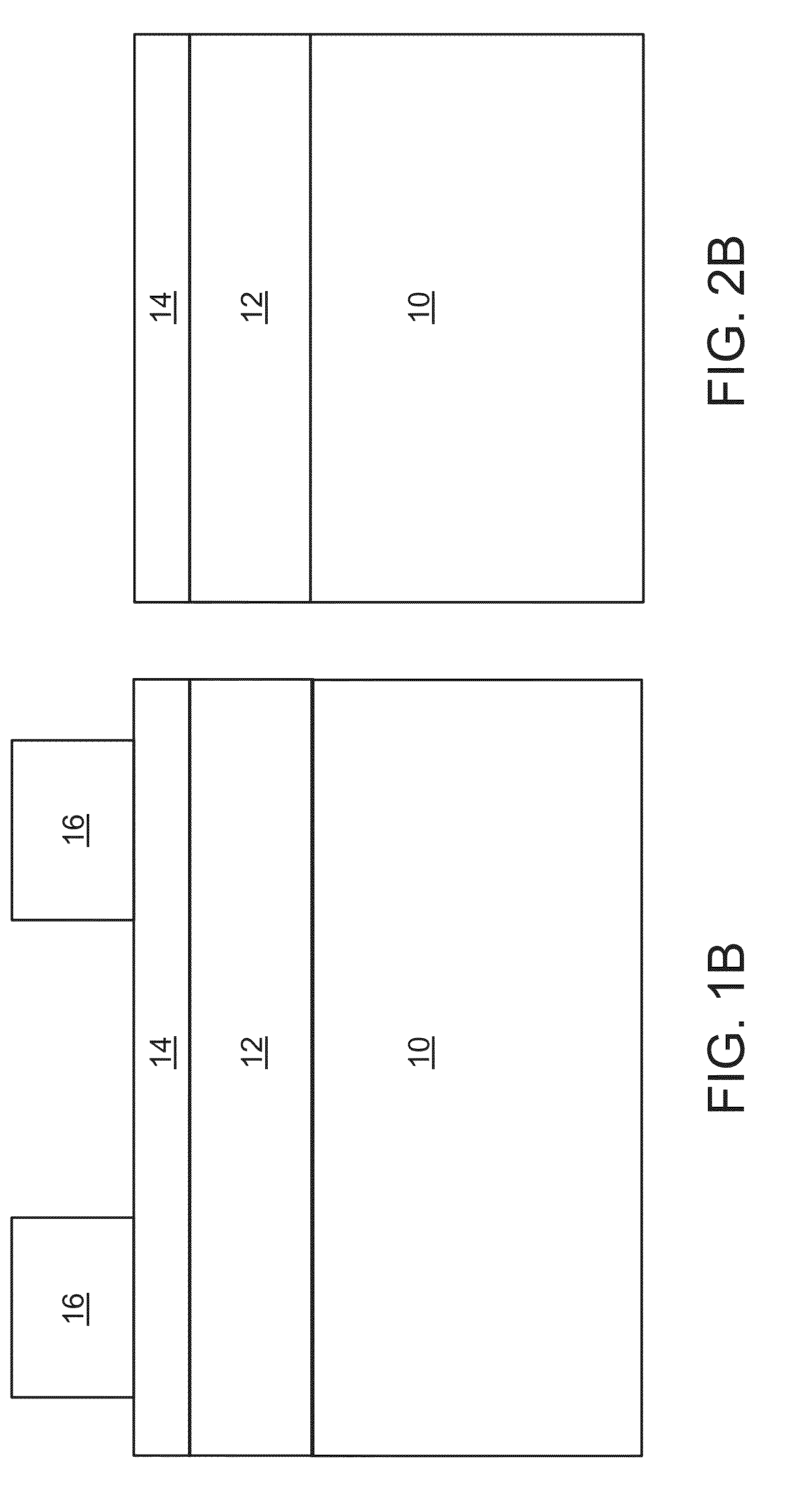
[0015]FIGS. 1A-1Y and 2A-2X are side cross sectional views showing the process steps in forming the Fin-FET split gate memory cell array. FIGS. 1A-1X show the cross section in the word line (X) direction, and FIGS. 2A-2X show the cross section in the bit line (Y) direction. The process begins by forming a layer of silicon nitride (“nitride”) 12 on the surface of a silicon substrate 10. A layer polysilicon (“poly”) 14 is formed on the nitride layer 12. A second nitride layer 16 is form...
PUM
 Abstract
Description
Claims
Application Information
 - R&D
- Intellectual Property
- Life Sciences
- Materials
- Tech Scout
- Unparalleled Data Quality
- Higher Quality Content
- 60% Fewer Hallucinations
Browse by: Latest US Patents, China's latest patents, Technical Efficacy Thesaurus, Application Domain, Technology Topic, Popular Technical Reports.
© 2025 PatSnap. All rights reserved.Legal|Privacy policy|Modern Slavery Act Transparency Statement|Sitemap|About US| Contact US: help@patsnap.com